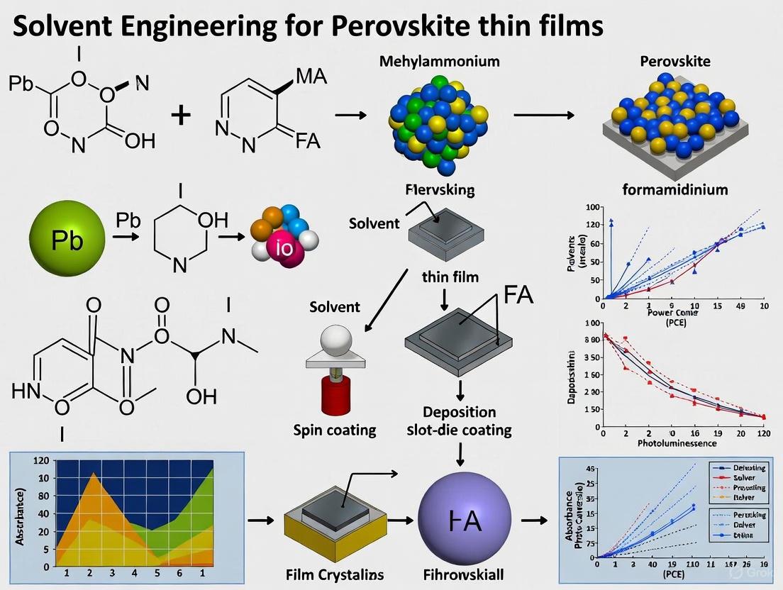
Solvent Engineering for High-Performance Perovskite Thin Films: Mechanisms, Methods, and Commercial Outlook
This article provides a comprehensive analysis of recent advances in solvent engineering for fabricating high-quality perovskite thin films, a cornerstone for efficient and stable perovskite solar cells (PSCs).
Solvent Engineering for High-Performance Perovskite Thin Films: Mechanisms, Methods, and Commercial Outlook
Abstract
This article provides a comprehensive analysis of recent advances in solvent engineering for fabricating high-quality perovskite thin films, a cornerstone for efficient and stable perovskite solar cells (PSCs). We explore the fundamental coordination chemistry between solvents and perovskite precursors, detailing how binary and ternary solvent systems control crystallization kinetics and intermediate phase formation. The review systematically covers scalable deposition methodologies, including blade and slot-die coating, and delves into advanced strategies for troubleshooting common defects and optimizing film morphology through anti-solvent and additive engineering. A critical comparison of solvent systems validates their impact on device performance and operational stability, supported by efficiency data and stability metrics from recent literature. This resource is tailored for researchers and scientists engaged in the development of next-generation perovskite photovoltaics and other optoelectronic devices.
The Chemistry of Control: Unraveling Solvent-Precursor Interactions and Crystallization Fundamentals
In the field of perovskite thin films research, solvent engineering is a critical lever for controlling film quality, crystallization kinetics, and ultimately, device performance. The foundational step in this process lies in the coordination chemistry between solvent molecules and the metal cations in perovskite precursors, particularly Pb²⁺ and Sn²⁺. The strength and nature of these coordination bonds directly influence the structure of precursor colloids, intermediate phases, and the final crystalline film. A precise understanding of these interactions enables researchers to rationally design solvent systems that suppress detrimental phases, promote uniform crystallization, and minimize defects. This Application Note details the specific coordination mechanisms of common solvents with Pb²⁺ and Sn²⁺, provides quantitative binding data, and outlines standardized protocols for investigating these interactions, framed within the broader thesis that mastering coordination chemistry is paramount for advancing perovskite research.
Fundamental Coordination Mechanisms
The binding of solvent molecules to Pb²⁺ and Sn²⁺ cations is a classic example of Lewis acid-base chemistry. The metal cations act as Lewis acids (electron pair acceptors), while solvent molecules with donor atoms (e.g., O, S, N) function as Lewis bases (electron pair donors). The coordination sphere formed around each cation determines the stability and reactivity of the precursor complex.
- Sn²⁺ vs. Pb²⁺ Coordination: Sn²⁺, with its higher effective nuclear charge and smaller ionic radius, is a stronger Lewis acid than Pb²⁺. This results in a greater thermodynamic driving force for coordination with Lewis basic solvents. However, the propensity of Sn²⁺ to oxidize to Sn⁴⁺ in the presence of coordinating species like dimethyl sulfoxide (DMSO) adds a layer of complexity not present with Pb²⁺ [1] [2].
- Common Coordination Modes: The most prevalent binding involves the donation of electron density from the oxygen atom of carbonyl-containing solvents (e.g., DMF, NMP) or the sulfur atom in DMSO to the vacant s and p orbitals of the metal cations. This forms a solvate complex that can significantly alter the evaporation kinetics and nucleation barrier of the perovskite material [2] [3].
- Role of Solvent Structure: The molecular structure of the solvent dictates its coordination capability. For instance, the open monoclinic crystal structure of SnI₂ allows bulkier solvent molecules to access and coordinate with the Sn²⁺ cation, whereas the compact layered structure of PbI₂ often permits only surface interactions [2].
Quantitative Analysis of Solvent-Cation Binding
The binding strength between solvents and cations can be quantified through various experimental and computational methods. The following table summarizes key quantitative data for common solvent-cation pairs relevant to perovskite processing.
Table 1: Quantitative Binding Parameters for Solvent Interactions with Pb²⁺ and Sn²⁺
| Solvent | Cation | Binding Energy (eV) | Observed Bond Length (Å) | Primary Binding Motif | Key Experimental Evidence |
|---|---|---|---|---|---|
| Dimethyl Sulfoxide (DMSO) | Sn²⁺ | - | - | S=O → Sn²⁺ coordination | FTIR peak shifts (C–S, S=O stretch) [2] |
| Dimethylformamide (DMF) | Sn²⁺ | - | - | C=O → Sn²⁺ coordination | FTIR, NMR chemical shifts [2] [3] |
| N-Methyl-2-pyrrolidone (NMP) | Pb²⁺ | - | - | C=O → Pb²⁺ coordination | Drives (100) orientation in intermediate phases [3] |
| Trichloromethane (TCM) | Sn²⁺ | -0.44 | - | Halogen (Cl–Sn) & Hydrogen bonding | FTIR (C–Cl shift: 772.5 to 763.5 cm⁻¹), ¹³C NMR (0.3 ppm shift) [2] |
| Trichloromethane (TCM) | Pb²⁺ | -0.26 | - | Weak Hydrogen bonding | Minimal FTIR/NMR shifts, weak interaction [2] |
The data reveals clear trends in solvent selectivity. DMSO and DMF show strong coordination with both cations but are integral to the conventional solvent system. A key finding is the selective and stronger coordination of TCM with Sn²⁺ compared to Pb²⁺, a phenomenon exploited to suppress Sn-rich colloids and improve stoichiometry in Sn-Pb mixed perovskite films [2].
Table 2: Impact of Solvent Coordination on Perovskite Film Properties
| Solvent System | Coordinating Strength | Impact on Precursor Colloids | Resulting Film Morphology | Device Performance (PCE) |
|---|---|---|---|---|
| DMF/DMSO (Binary) | Moderate, non-selective | Sn-rich colloids at high concentration | Sn segregation, inhomogeneous | 17.5% ± 1.7% (Baseline) [2] |
| DMF/DMSO/TCM (Ternary) | Strong, Sn²⁺-selective | Stoichiometric, well-dispersed colloids | Uniform, reduced Sn segregation | 20.3% ± 0.6% (Single-junction) [2] |
| DMF/NMP | Promotes Pb²⁺ intermediates | - | Preferentially (100)-oriented films | 25.33% (Optimized device) [3] |
Experimental Protocols
This section provides detailed methodologies for key experiments used to probe solvent-cation interactions.
Protocol: Fourier-Transform Infrared (FTIR) Spectroscopy for Binding Motif Analysis
Objective: To identify the functional groups involved in solvent-cation coordination and characterize the binding motif (e.g., halogen vs. hydrogen bonding).
- Sample Preparation:
- Prepare saturated solutions of the metal halide (e.g., SnI₂ or PbI₂) in the solvent of interest (e.g., TCM).
- Prepare a pure solvent sample as a reference.
- Instrument Setup:
- Use an FTIR spectrometer equipped with a liquid cell (e.g., with KBr windows).
- Set a resolution of 2 cm⁻¹ and accumulate 32 scans per spectrum over a range of 4000-400 cm⁻¹.
- Data Acquisition:
- Collect the background spectrum with an empty cell or a cell filled with a non-coordinating solvent.
- Acquire spectra for the pure solvent and the metal halide solution.
- Data Analysis:
- Overlay the spectra and identify key vibrational peaks (e.g., C=O stretch ~1650-1700 cm⁻¹, S=O stretch ~1050 cm⁻¹, C–Cl stretch ~750-800 cm⁻¹).
- A shift in the peak position (e.g., C–Cl stretch shifting from 772.5 cm⁻¹ in pure TCM to 763.5 cm⁻¹ in a SnI₂-TCM solution) indicates coordination and electron density redistribution [2].
Protocol: Nuclear Magnetic Resonance (NMR) Spectroscopy for Quantifying Interaction Strength
Objective: To quantify the electron density changes upon coordination, providing a measure of interaction strength.
- Sample Preparation:
- Dissolve individual perovskite precursor components (e.g., FAI, SnI₂, PbI₂) in a deuterated solvent (e.g., DMSO-d6).
- Add a controlled volume (e.g., 10 vol%) of the solvent under investigation (e.g., TCM) to each solution.
- Instrument Setup:
- Use a high-resolution NMR spectrometer (e.g., 400 MHz or higher).
- For ¹³C NMR, ensure adequate signal-to-noise through sufficient scans.
- Data Acquisition:
- For each sample, acquire ¹H and ¹³C NMR spectra.
- Calibrate the chemical shift scale using the deuterated solvent peak.
- Data Analysis:
- Compare the chemical shift (δ) of the carbon atoms in the test solvent across different solutions.
- A significant downfield shift (e.g., 0.3 ppm for TCM in the presence of SnI₂ compared to ~0.1 ppm with PbI₂) indicates deshielding due to reduced electron density, confirming a stronger coordination interaction [2].
Protocol: Density Functional Theory (DFT) Calculations for Binding Energy
Objective: To computationally determine the binding energy and optimal geometry of solvent-cation complexes.
- Model Construction:
- Build initial molecular models of the solvent molecule and the metal halide unit (e.g., SnI₂ or PbI₂).
- Computational Details:
- Use a DFT package like Gaussian 09.
- Select an appropriate functional and basis set (e.g., PBE, TPSS, or B3LYP with a 6-31+G(d,p) basis set for light atoms and LanL2DZ for Pb and I).
- Include solvent effects implicitly using a polarizable continuum model (e.g., IEF-PCM for water, ε = 78.4) [4].
- Geometry Optimization:
- Fully optimize the geometry of the isolated molecules and the proposed complex without symmetry constraints.
- Confirm the optimized structure is a true minimum on the potential energy surface by performing a frequency calculation (no imaginary frequencies).
- Energy Calculation:
- Calculate the single-point energy for the optimized complex and the isolated monomers.
- Compute the binding energy (ΔEbind) as: ΔEbind = E(complex) - [E(solvent) + E(metal halide)].
- A more negative value indicates a more stable complex (e.g., -0.44 eV for SnI₂-TCM vs. -0.26 eV for PbI₂-TCM) [2].
Visualization of Coordination Structures and Workflows
The following diagrams illustrate key coordination environments and experimental workflows.
SnI₂-Trichloromethane Coordination Structure
Diagram Title: Sn²⁺ Coordination with TCM
Solvent-Cation Binding Analysis Workflow
Diagram Title: Experimental Workflow for Binding Analysis
The Scientist's Toolkit: Essential Research Reagents
Table 3: Key Reagents for Studying Solvent-Cation Coordination
| Reagent | Function/Role in Coordination Chemistry | Example Use Case |
|---|---|---|
| Dimethyl Sulfoxide (DMSO) | Strong Lewis base coordinates via S=O group; forms intermediate phases. | Standard component in binary solvent systems for coordinating both Pb²⁺ and Sn²⁺ [2] [3]. |
| N-Methyl-2-pyrrolidone (NMP) | Lewis base coordinates via C=O group; templates specific crystal orientations. | Used in DMF/NMP systems to promote (100)-oriented perovskite films [3]. |
| Trichloromethane (TCM) | Selective solvent coordinates via Cl–Sn bond and H-bonding; suppresses Sn-rich colloids. | Additive in ternary solvent systems to preferentially coordinate Sn²⁺ and improve stoichiometry [2]. |
| Cyclohexylamine (CHA) | Additive that interacts with crystal facets to influence growth kinetics and orientation. | Used in SACR strategy with DMF/DMSO to obtain homogeneous (111)-oriented films [3]. |
| Cyclohexylamine Iodide (CHAI) | Additive that bonds selectively with specific crystal nuclei to control facet growth. | Used in SACR strategy with DMF/NMP to obtain homogeneous (100)-oriented films [3]. |
In the solution-processing of perovskite thin films, the formation of crystalline intermediate phases is a critical step that dictates the final film's morphology, grain size, and optoelectronic quality. The solvents used in the precursor ink, particularly dimethyl sulfoxide (DMSO), N,N'-dimethylformamide (DMF), and N-methyl-2-pyrrolidone (NMP), are not inert mediums but active components that coordinate with lead halide precursors to direct crystal growth. This application note delineates the distinct roles of these solvents in intermediate phase formation and provides detailed protocols for leveraging their properties to fabricate high-performance perovskite solar cells.
Solvent Properties and Coordination Chemistry
The efficacy of a solvent in directing perovskite crystal growth is governed by its Lewis basicity, coordination capability, and volatility. These properties determine the stability and composition of the intermediate phases formed during the initial film deposition.
Table 1: Key Properties of Common Perovskite Processing Solvents
| Solvent | Lewis Donor Number (kcal/mol) | Boiling Point (°C) | Primary Role in Intermediate Phase | Impact on Crystal Growth |
|---|---|---|---|---|
| DMSO | 29.8 [5] | 189 | Forms highly stable, often one-dimensional, coordination complexes with PbI₂ (e.g., MA₂Pb₃I₈·5DMSO) [6]. | Slows crystallization, promotes large, monolithic grains via a lateral growth mechanism [7]. |
| DMF | 26.6 [5] | 153 | Forms less stable complexes with PbI₂ compared to DMSO. Often used in binary mixtures with DMSO [8]. | Higher volatility can lead to faster crystallization, often resulting in smaller grains if not controlled. |
| NMP | 27.3 [5] | 202 | Acts as a moderating agent; can subtly decouple DMSO-related complexes, balancing coordination and supersaturation [8]. | Promotes rapid α-phase nucleation and controllable crystal growth, minimizing interfacial voids [8]. |
The fundamental interaction involves the Lewis acidic Pb²⁺ ion and the carbonyl oxygen of DMF and NMP or the sulfoxide oxygen of DMSO. The strength of this coordinate bond is proportional to the solvent's Lewis basicity, explaining the trend in intermediate phase stability: DMSO > NMP > DMF [5] [9]. This coordinated framework templates the subsequent perovskite structure upon thermal annealing or antisolvent exposure.
Visualizing the Crystallization Pathways
The following diagram illustrates the distinct crystallization pathways directed by different solvent systems, from precursor solution to final perovskite film.
Experimental Protocols
Protocol: Intermediate Phase Formation and Crystal Growth for High-Efficiency Solar Cells
This protocol is adapted from methodologies that yield monolithic, large-grained perovskite films via lateral crystal growth, essential for high photovoltaic performance [7].
Objective: To prepare a high-quality
Cs₀.₁FA₀.₉PbI₃perovskite film with monolithic grain structure using a DMF/DMSO solvent system and potassium halide additives.Materials:
- Precursor Salts: FAI (1.0 M), PbI₂ (1.1 M), CsI (0.1 M)
- Solvents: Anhydrous DMF, Anhydrous DMSO
- Additive: KCl (5 mol% relative to PbI₂)
- Anti-solvent: Chlorobenzene (CB) or Diethyl ether
Procedure:
- Precursor Ink Formulation: Dissolve the precursor salts and KCl additive in a mixed solvent of DMF:DMSO (4:1, v/v). Stir at 60°C for 2–4 hours until completely dissolved.
- Film Deposition: Spin-coat the precursor solution onto a pre-heated (≈70°C) mesoporous TiO₂-coated substrate at 4000 rpm for 25 seconds.
- Anti-solvent Quenching: At 5–7 seconds before the end of the spin-coating program, rapidly drip 200 µL of chlorobenzene onto the center of the spinning substrate. This step initiates the formation of the intermediate phase.
- Intermediate Phase Characterization: The film will appear translucent or brownish. XRD analysis at this stage should show characteristic peaks of the solvent-coordinated intermediate phase (e.g., a peak at ~8.5° 2θ for a DMSO-based complex), confirming successful formation prior to annealing.
- Thermal Annealing: Immediately transfer the film to a hotplate and anneal at 100°C for 45–60 minutes. Observe a color change to dark brown, indicating perovskite crystallization.
- Growth Direction Analysis: Use in-situ GIWAXS or post-mortem SEM cross-sectional analysis to confirm a lateral (Type III) growth pattern, which is associated with high-efficiency devices [7].
Protocol: Scalable Blade-Coating with NMP-Modified Ink
This protocol is designed for scalable fabrication of perovskite films, where controlling crystallization kinetics without anti-solvent is critical [8].
Objective: To fabricate a pinhole-free, large-area
FA₀.₈₅MA₀.₁Cs₀.₀₅PbI₃perovskite film via vacuum-assisted blade-coating using an NMP-modified ink.Materials:
- Precursor Salts: FAI, MABr, CsI, PbI₂, PbBr₂
- Solvents: Anhydrous DMF, Anhydrous DMSO, Anhydrous NMP
- Substrate: Textured or flat silicon, ITO/glass
Procedure:
- Ink Reformulation: Prepare the precursor solution in a mixed solvent of DMF:DMSO:NMP (e.g., 4:1:0.25, v/v/v). The addition of a small volume of NMP is crucial for decoupling strong DMSO complexes and balancing the supersaturation rate during vacuum quenching [8].
- Blade-Coating: Deposit the ink onto a substrate maintained at 25–30°C using a blade coater with a fixed gap (e.g., 100–200 µm).
- Vacuum Quenching: Immediately after coating, place the wet film in a vacuum chamber (≈10 kPa) for 30–60 seconds to uniformly extract solvents and induce supersaturation.
- Thermal Annealing: Transfer the film to a hotplate and anneal at 100°C for 10 minutes. The presence of NMP facilitates a void-free buried interface by moderating the drying front.
- Quality Control: Perform SEM on the final film's surface and buried interface. The film should be dense, with large grains and an absence of voids at the substrate interface, confirming the success of the solvent engineering strategy.
The Scientist's Toolkit: Essential Research Reagents
Table 2: Key Reagents for Investigating Solvent-Directed Intermediate Phases
| Reagent / Material | Function / Role | Application Notes |
|---|---|---|
| Dimethyl Sulfoxide (DMSO) | Forms highly stable, 1D intermediate phases with PbI₂ (e.g., MA₂Pb₃I₈·5DMSO), dramatically retarding crystallization to enable large grains [7] [6]. | Use in binary mixtures with DMF (e.g., 4:1 v/v DMF:DMSO). Strong coordination can trap solvent; requires effective removal during annealing. |
| N-Methyl-2-Pyrrolidone (NMP) | Moderating agent that balances supersaturation rate and coordination strength. Subtly decouples DMSO complexes, preventing void formation at the buried interface [8]. | Optimal as a minor additive (e.g., 5% v/v of total solvent) to DMF/DMSO mixtures for scalable blade-coating. |
| Chlorobenzene (CB) | Anti-solvent for quenching during spin-coating. Rapidly reduces precursor solubility, triggering the formation of a coordinated intermediate film [7]. | Dripping timing is critical. Typically applied 5-15 seconds before the end of the spin cycle. |
| Potassium Chloride (KCl) | Crystallization additive. Does not incorporate into the 3D perovskite lattice but passivates defects at grain boundaries, suppressing J-V hysteresis and facilitating monolithic grain growth [7]. | Use at low concentrations (1-5 mol% relative to Pb). |
| Lead Iodide (PbI₂) | Primary inorganic perovskite precursor. Acts as a Lewis acid to form coordination complexes with aprotic solvents [5] [9]. | Often used in a slight stoichiometric excess (e.g., 1.05-1.10 molar ratio to FA/MAI) to ensure full conversion and passivate defects. |
Strategic solvent engineering using DMSO, DMF, and NMP provides powerful levers to control the crystallization of perovskite films. DMSO directs growth through stable intermediate phases, while NMP fine-tunes this process for scalable techniques. The protocols and data herein provide a framework for exploiting these solvent interactions to achieve reproducible, high-performance optoelectronic devices.
The pursuit of high-performance, commercially viable perovskite photovoltaics is intrinsically linked to the quality of the perovskite absorber layer, which is a direct consequence of the precursor ink properties and the subsequent crystallization process. For tin-lead (Sn-Pb) narrow-bandgap perovskites, which are essential for high-efficiency all-perovskite tandem solar cells, achieving micron-thick, uniform films is paramount for optimal near-infrared photon absorption. However, a significant roadblock exists: the formation of Sn-rich colloidal aggregates in high-concentration precursor solutions. These aggregates originate from the insufficient coordination of tin(II) iodide (SnI₂) in conventional solvent systems, leading to non-uniform crystallization, stoichiometric imbalance, limited carrier diffusion lengths, and pronounced Sn segregation at the film surface [2]. This application note details advanced protocols for analyzing precursor ink properties and outlines effective strategies to suppress Sn-rich phase formation, thereby enabling the fabrication of high-quality perovskite films.
Quantitative Analysis of Precursor Ink Properties
The following tables summarize key quantitative data essential for diagnosing and understanding colloidal behavior in perovskite precursor inks.
Table 1: Key Findings from Colloidal Analysis of Sn-Pb Perovskite Inks
| Analysis Technique | Observation | Interpretation & Implication |
|---|---|---|
| Photoluminescence (PL) Spectroscopy | Consecutive redshift in PL peak with increasing precursor concentration in binary DMF/DMSO system [2]. | Indicates formation of Sn-rich colloids at higher concentrations, a root cause of inhomogeneous films. |
| Dynamic Light Scattering (DLS) | Bimodal hydrodynamic particle size distribution. TCM addition shifts small-cluster peak to lower size and large-aggregate peak to higher size [2]. | TCM breaks large aggregates, releasing dispersed precursor units and fostering more uniform nucleation and growth. |
| Fourier-Transform Infrared (FTIR) Spectroscopy | Shifts in C–Cl and C–H vibration peaks for SnI₂ in TCM [2]. | Confirms TCM coordinates with SnI₂ via halogen and hydrogen bonding. |
| NMR Studies (¹³C) | Largest downfield shift (0.3 ppm) of TCM carbon signal when mixed with SnI₂ [2]. | Demonstrates the strongest selective interaction between TCM and SnI₂ compared to other perovskite components. |
| DFT Calculations | Binding energy of -0.44 eV for SnI₂–TCM vs. -0.26 eV for PbI₂–TCM [2]. | Quantifies stronger thermodynamic driving force for TCM coordination with SnI₂, explaining its efficacy. |
Table 2: Performance Outcomes of Engineered Solvent Systems
| Parameter | Conventional Binary Solvent (DMF/DMSO) | Engineered Ternary Solvent (DMF/DMSO/TCM) |
|---|---|---|
| Carrier Diffusion Length | Limited | ~11 μm [2] |
| Single-Junction Solar Cell Efficiency | Insufficient for thick films | 24.2% [2] |
| All-Perovskite Tandem Solar Cell Efficiency | Insufficient for thick films | 29.3% [2] |
| Sn Segregation | Pronounced | Significantly reduced [2] |
| Film Morphology | Non-uniform, dendritic structures, voids [2] | Uniform, dense, pinhole-free [2] |
Experimental Protocols
Protocol 1: Analyzing Colloidal Properties in Precursor Inks
This protocol outlines methods to characterize the colloidal state of Sn-Pb perovskite precursor inks.
1.0 Materials
- Perovskite precursor solution (e.g., Sn-Pb iodide/ bromide salts with organic cations in desired solvent).
- Spectrophotometer cuvettes.
- Dynamic Light Scattering (DLS) instrument.
- Fluorometer.
2.0 Photoluminescence (PL) Spectroscopy of Precursor Solutions 1. Preparation: Place the precursor solution in a quartz cuvette. 2. Measurement: Acquire PL emission spectra at a fixed excitation wavelength. 3. Analysis: Monitor the peak position and intensity. A redshift in the PL peak indicates the formation of Sn-rich colloids, while a blueshift upon additive introduction suggests a more balanced Sn/Pb ratio in the colloids [2].
3.0 Dynamic Light Scattering (DLS) Measurements 1. Preparation: Filter the precursor solution with an appropriate syringe filter to remove dust. 2. Measurement: Load the filtered solution into a DLS sample cell and measure the intensity autocorrelation function. 3. Analysis: Analyze the data to obtain the hydrodynamic size distribution. A bimodal distribution is typical, with shifts in peak sizes and intensities indicating changes in aggregate and cluster populations [2].
4.0 UV-Vis Absorption Spectroscopy 1. Preparation: Dilute the precursor ink if necessary to remain within the spectrophotometer's linear range. 2. Measurement: Record the absorption spectrum. 3. Analysis: Compare absorption profiles to assess the dissolution efficiency of individual components (e.g., SnI₂) in different solvents [2].
Protocol 2: Fabricating Micron-Thick Sn-Pb Films via Ternary Solvent Engineering
This protocol describes a method to fabricate high-quality, thick Sn-Pb perovskite films by employing a ternary solvent system to control colloidal chemistry.
1.0 Materials
- Precursor Salts: SnI₂, PbI₂, FAI, MAI, CsI.
- Solvents: Dimethylformamide (DMF), Dimethyl sulfoxide (DMSO), Trichloromethane (TCM).
- Substrate: Patterned ITO/glass.
- Antisolvent: Anhydrous chlorobenzene or diethyl ether.
2.0 Precursor Ink Formulation 1. Solution Preparation: Co-dissolve the precursor salts in a mixed solvent of DMF:DMSO:TCM (e.g., 0.75:0.2:0.05 by volume) to achieve a total precursor concentration of ~2.4 M [2]. 2. Stirring: Stir the mixture at 60°C for 2-4 hours until a clear, homogeneous solution is obtained.
3.0 Film Deposition and Crystallization 1. Deposition: Spin-coat the precursor solution onto the pre-cleaned substrate. 2. Antisolvent Quenching: During the final stage of spin-coating, apply an antisolvent (e.g., chlorobenzene) to initiate uniform nucleation. 3. Annealing: Transfer the film to a hot plate and anneal at ~100°C for 10-20 minutes to form a crystalline, black perovskite film.
4.0 Critical Step for Printed Films: Gas-Pulse Triggered Crystallization For scalable deposition techniques like slot-die coating where antisolvent quenching is impractical, an alternative crystallization trigger is required [10]. 1. Coating: Slot-die coat the precursor solution (e.g., FAI and SnI₂ in DMF:tBP 6:4 v/v) onto a heated substrate. 2. Gas Pulse: During the metastable phase of the liquid film, apply a short pulse of inert gas (N₂) to the wet film surface. The timing of this pulse is critical and must be optimized [10]. 3. Annealing: Complete the crystallization by annealing on a hot plate.
Workflow Visualization: From Problem to Solution
The following diagram illustrates the logical pathway from identifying the problem of Sn-rich aggregates to implementing the ternary solvent solution and achieving high-performance devices.
The Scientist's Toolkit: Essential Research Reagents
Table 3: Key Reagent Solutions for Sn-Pb Perovskite Ink Research
| Reagent / Material | Function / Role | Key Consideration |
|---|---|---|
| Trichloromethane (TCM) | Coordination solvent in ternary system; selectively bonds with SnI₂ to suppress Sn-rich colloid formation [2]. | Prefer anhydrous grade. Its high volatility ensures easy removal during annealing, minimizing residue. |
| 4-(tert-butyl)pyridine (tBP) | Complexing agent/co-solvent that slows down Sn perovskite crystallization by forming stable intermediate phases [10]. | Replaces oxidative DMSO, offering a broader processing window, especially for printing. |
| SnF₂ / SnCl₂ Additives | Common additives that create a Sn-rich environment to compensate for Sn vacancy (Vₛₙ) defects and mitigate Sn²⁺ oxidation [10]. | SnCl₂ can lead to surface segregation of Cl⁻, influencing energy level alignment [10]. |
| MASnCl₃ Additive | A perovskite-structured additive that modulates crystallization kinetics, offering an intermediate rate between SnCl₂ and MACl [10]. | Synthesized by mixing equimolar MACl and SnCl₂. Promotes compact, pinhole-free films in printed devices. |
| Cyclohexylamine (CHA) / CHAI | Additives for facet orientation control in two-step methods; influence crystal growth via facet-selective bonding [3]. | Used in solvent-additive cascade regulation (SACR) strategies to achieve homogeneous (111) or (100) orientations. |
Controlling the colloidal properties of precursor inks is not merely a preliminary step but a fundamental aspect of fabricating high-performance Sn-Pb perovskite solar cells. The formation of Sn-rich aggregates in conventional solvent systems is a critical barrier to achieving high-quality, micron-thick films. As detailed in these application notes, the implementation of a ternary solvent system incorporating TCM effectively addresses this by providing selective coordination for SnI₂. When combined with robust analytical protocols for ink characterization and optimized deposition techniques, this strategy paves the way for the realization of efficient and stable single-junction and tandem perovskite photovoltaics, directly supporting the broader thesis that solvent engineering is pivotal to advancing perovskite thin-film research.
Solvent engineering plays a pivotal role in controlling the crystallization kinetics and final film quality of metal halide perovskites. While binary solvent systems have been the conventional choice for perovskite precursor formulations, their limitations in achieving homogeneous crystallization in thick films or scalable deposition processes have become apparent. Ternary solvent systems have emerged as a sophisticated strategy to overcome these challenges by providing enhanced coordination chemistry, particularly with tin-based perovskites where oxidation and segregation pose significant obstacles to device performance and stability. This application note delineates the fundamental principles, experimental evidence, and practical protocols for implementing ternary solvent systems to suppress cation segregation and improve coordination in perovskite thin films.
Comparative Analysis: Binary vs. Ternary Solvent Systems
Fundamental Mechanisms and Performance Outcomes
Table 1: Comparative Analysis of Binary and Ternary Solvent Systems in Perovskite Processing
| Characteristic | Binary Solvent System (e.g., DMF/DMSO) | Ternary Solvent System (e.g., DMF/DMSO/TCM) |
|---|---|---|
| Coordination Chemistry | Under-coordination of SnI₂ at high concentrations leading to Sn-rich colloids [11] | Full coordination with SnI₂ via halogen and hydrogen bonding, suppressing Sn-rich phases [11] |
| Precursor Colloids | Bimodal size distribution with Sn-rich aggregates causing non-stoichiometry [11] | Modified colloidal distribution with reduced Sn-rich aggregates and more dispersed precursor units [11] |
| Crystallization Behavior | Non-uniform crystallization with Sn segregation at surfaces [11] | Uniform nucleation and reduced Sn segregation [11] |
| Film Morphology | Inhomogeneous films with limited carrier diffusion lengths [11] | Stoichiometric micron-thick films with carrier diffusion lengths of ~11 μm [11] |
| Device Performance | Single-junction: <24.2%; Tandem: <29.3% [11] | Single-junction: 24.2%; Tandem: 29.3% [11] |
| Coordination Binding Energy | Limited SnI₂ coordination [11] | Strong SnI₂-TCM binding (-0.44 eV vs. -0.26 eV for PbI₂) [11] |
| Scalability Compatibility | Limited in vacuum-assisted blade coating [8] | Improved compatibility with scalable methods [8] |
Hydrogen Bonding in Ternary Solvent Systems
Ternary solvent engineering incorporating hydrogen bonding has demonstrated significant advantages for formamidinium lead triiodide (FAPbI₃) perovskite solar cells. The introduction of anisole (AN) as a third solvent component creates hydrogen bonds with DMF and DMSO solvents through the lone electron pairs on the -O- atom. These hydrogen bonds effectively delay solvent evaporation, which controls crystal growth rate and enables significant improvements in both grain size and film surface roughness [12].
The hydrogen bonding within the ternary solvent system increases the grain size from approximately 400 nm in binary systems to over 800 nm in ternary systems, while simultaneously reducing surface roughness from 46.2 nm to 29.1 nm. These morphological improvements translate directly to enhanced device performance, with power conversion efficiency increasing from 12.23% for binary systems to 13.85% for ternary systems incorporating AN [12].
Underlying Coordination Mechanisms
Molecular-Level Interactions
The enhanced performance of ternary solvent systems originates from specific molecular-level interactions that improve precursor coordination chemistry:
Selective Coordination: In the DMF/DMSO/TCM ternary system, TCM preferentially coordinates with SnI₂ while minimally affecting PbI₂, as confirmed through absorption spectroscopy and ¹H NMR [11]. This selective interaction addresses the fundamental imbalance in crystallization rates between Sn and Pb components.
Binding Energy Differential: DFT calculations reveal a significant binding energy differential between SnI₂-TCM (-0.44 eV) and PbI₂-TCM (-0.26 eV) complexes [11]. This differential enables selective modulation of crystallization kinetics.
Structural Penetration: The monoclinic structure of SnI₂ allows TCM to insert into the layers, forming Cl-Sn bonds with exposed Sn²⁺ sites and hydrogen bonds with iodide ions. In contrast, PbI₂'s compact layered hexagonal structure only permits weak hydrogen bonding [11].
Charge Transfer Effects: Planar charge difference analysis demonstrates a fivefold greater charge transfer in the SnI₂-TCM system compared to PbI₂-TCM, explaining the stronger coordination capability [11].
Crystallization Kinetics Modulation
The introduction of a third solvent component fundamentally alters the crystallization pathway by:
Nucleation Control: Optical microscopy studies reveal that ternary solvent systems promote more uniform nucleation density compared to binary systems, which exhibit sparse nucleation sites [11].
Intermediate Phase Engineering: Strongly coordinating solvents like DMSO form intermediate phases that retard crystallization, but can become trapped, leading to void formation at the perovskite/substrate interface, particularly in scalable deposition processes [8].
Supersaturation Management: The addition of NMP in ternary formulations for blade coating creates a balanced trade-off between supersaturation rate and coordination capability, enabling rapid α-phase perovskite nucleation together with controllable crystal growth [8].
Experimental Protocols
Protocol 1: Ternary Solvent System for Tin-Lead Perovskites
This protocol details the preparation of micron-thick Sn-Pb perovskite films using the DMF/DMSO/TCM ternary solvent system for enhanced coordination and suppressed phase segregation [11].
Materials and Equipment
Table 2: Essential Research Reagent Solutions
| Reagent | Function | Specifications |
|---|---|---|
| SnI₂ | Perovskite precursor | 99.999% purity, store in inert atmosphere |
| PbI₂ | Perovskite precursor | 99.99% purity |
| Formamidinium Iodide (FAI) | Organic cation source | 99.99% purity |
| Dimethylformamide (DMF) | Primary solvent | Anhydrous, 99.8% |
| Dimethyl Sulfoxide (DMSO) | Coordinating solvent | Anhydrous, ≥99.9% |
| Trichloromethane (TCM) | Third solvent component | Anhydrous, 99.8% |
| Anisole | Antisolvent | Anhydrous, 99.7% |
Step-by-Step Procedure
Precursor Solution Preparation:
- Prepare a 2.4 M perovskite precursor solution in a nitrogen-filled glovebox (O₂ & H₂O < 0.1 ppm)
- Use solvent ratio DMF/DMSO/TCM = 4:1:0.5 (v/v/v)
- Dissolve SnI₂, PbI₂, and FAI in the ternary solvent mixture
- Stir overnight at room temperature to ensure complete dissolution and complex formation
Substrate Preparation:
- Clean glass/FTO substrates sequentially with acetone, isopropanol, and UV-ozone treatment
- Deposit appropriate electron or hole transport layers as required by device architecture
Film Deposition:
- Spin-coat the precursor solution using a two-step program: 1000 rpm for 10 s (acceleration 500 rpm/s) followed by 3000 rpm for 60 s
- At 50 s into the second step, apply 200 μL anisole antisolvent via pipette, delivered 1-1.5 cm above the substrate
- Complete the spin-coating process immediately after antisolvent application
Thermal Annealing:
- Transfer the substrate immediately to a hotplate at 100°C
- Anneal for 10 minutes in ambient conditions
- Allow to cool to room temperature before further processing
Characterization and Quality Control
- Film Thickness: Verify ~1.1 μm thickness using profilometry
- Morphology: Examine using SEM for pinhole-free, uniform coverage
- Optical Properties: Measure absorption spectrum and photoluminescence
- Elemental Distribution: Analyze Sn/Pb ratio using EDX or XPS to confirm homogeneous distribution
Protocol 2: Hydrogen-Bonding Ternary System for FAPbI₃
This protocol utilizes anisole as a hydrogen-bonding third solvent for improved FAPbI₃ film morphology [12].
Materials Preparation
- Prepare PbI₂ precursor solution with DMF/DMSO/AN ratio of 4:1:0.3 (v/v/v)
- Dissolve PbI₂ powder in the ternary solvent mixture with stirring for 12 hours
- Prepare separate FAI solution in isopropanol (concentration: 20 mg/mL)
Sequential Deposition Process
PbI₂ Layer Formation:
- Spin-coat PbI₂ precursor solution onto mesoporous TiO₂ substrate at 3000 rpm for 30 s
- Anneal at 70°C for 1 minute to remove excess solvent
Perovskite Conversion:
- Spin-coat FAI solution onto the PbI₂ layer at 3000 rpm for 30 s
- Anneal at 150°C for 30 minutes to form the FAPbI₃ perovskite structure
Device Completion:
- Cool samples to room temperature
- Proceed with hole transport layer and electrode deposition as required
Quality Assessment
- Verify large grain size (>800 nm) using SEM
- Measure surface roughness (<30 nm) using AFM
- Confirm α-phase formation and δ-phase suppression using XRD
Protocol 3: Scalable Blade Coating with Ternary Solvents
This protocol adapts ternary solvent systems for scalable blade coating processes [8].
Ink Formulation Optimization
- Prepare FA₀.₈₅MA₀.₁Cs₀.₀₅PbI₃ perovskite composition
- Use DMF/DMSO/NMP solvent ratio 4:1:0.25 (v/v/v)
- Stir precursor solution for 4 hours at 60°C
Blade Coating Parameters
- Substrate temperature: 30°C
- Blade height: 200 μm
- Coating speed: 10 mm/s
- Immediately transfer coated substrate to vacuum chamber
Vacuum Quenching
- Apply vacuum (10⁻² mbar) for 60 s to extract solvents
- Transfer to hotplate and anneal at 100°C for 10 minutes
- Characterize for void-free buried interface and large grain morphology
Advanced Applications and Scalability
Performance in Tandem Solar Cells
The implementation of ternary solvent systems has yielded remarkable improvements in all-perovskite tandem solar cells. The enhanced Sn-Pb absorber layers achieved through ternary solvent engineering enable efficiencies of 24.2% in single-junction cells and 29.3% in tandem devices, along with significantly improved long-term operational stability [11]. These performance gains stem directly from the improved carrier diffusion lengths of approximately 11 μm in micron-thick films, which enable enhanced near-infrared photon absorption in the narrow-bandgap subcells.
Scalable Manufacturing Compatibility
Ternary solvent systems demonstrate particular advantages in scalable deposition techniques beyond laboratory-scale spin coating:
Blade Coating: The addition of NMP to DMF/DMSO formulations enables superior film quality in blade-coated perovskites, achieving efficiencies of 25.38% for small-area cells (0.09 cm²) and 23.22% for mini-modules (21.84 cm²) [8].
Vacuum Compatibility: Ternary systems facilitate improved solvent extraction under vacuum quenching conditions, preventing the entrapped solvent issues that plague binary systems in scalable processes [8].
Crystallization Control: The balanced supersaturation rate and coordination capability in ternary solvents promote rapid α-phase nucleation with controllable crystal growth, essential for large-area uniformity [8].
Troubleshooting and Optimization Guidelines
Common Challenges and Solutions
Incomplete Coordination: If Sn segregation persists, increase the ratio of the third solvent component (TCM or AN) by 0.1-0.2 volume increments while maintaining overall precursor concentration.
Poor Film Morphology: For pinhole formation, optimize the antisolvent dripping timing and ensure consistent delivery height and speed.
Low Efficiency Devices: Verify solvent purity and SnI₂ freshness, as oxidation precursors diminish coordination effectiveness. Implement strict inert atmosphere handling.
Quality Control Metrics
Table 3: Key Quality Assessment Parameters
| Parameter | Target Value | Characterization Technique |
|---|---|---|
| Sn/Pb Ratio Uniformity | <5% variation across film | EDX mapping |
| Carrier Diffusion Length | >10 μm for Sn-Pb perovskites | TRPL or SPCM |
| Film Thickness | Target ±5% uniformity | Profilometry |
| Grain Size | >800 nm for FAPbI₃ | SEM analysis |
| Surface Roughness | <30 nm RMS | AFM |
| Sn⁴+ Content | <2% of total Sn | XPS analysis |
Ternary solvent systems represent a significant advancement in perovskite processing technology, addressing fundamental limitations of binary systems through enhanced coordination chemistry and selective solute-solvent interactions. The protocols outlined herein provide researchers with practical methodologies for implementing these systems across various perovskite compositions and deposition techniques. The demonstrated improvements in film morphology, compositional homogeneity, and device performance underscore the critical importance of solvent engineering in advancing perovskite photovoltaics toward commercial viability.
From Lab to Fab: Solvent Engineering in Scalable Deposition and Advanced Formulations
Solvent engineering is a cornerstone technique in the fabrication of high-performance perovskite solar cells (PSCs). The quality of the perovskite thin film, with its direct impact on photovoltaic parameters, is predominantly dictated by the precise control of crystallization dynamics during solution processing. This application note details optimized protocols for spin-coating, focusing on advanced solvent engineering and antisolvent quenching techniques, to enable the reproducible fabrication of perovskite films with large, monolithic grains and superior optoelectronic properties. The methodologies outlined herein are contextualized within the broader research framework of modulating precursor-solvent interactions and crystallization kinetics to suppress deleterious phase segregation and defect formation, particularly in technologically relevant tin-lead (Sn-Pb) and formamidinium-cesium (FA-Cs) based perovskite systems [13] [14] [15].
Solvent Engineering: Fundamentals and Protocols
The Challenge of Sn-Pb Perovskites and Ternary Solvent Systems
A significant challenge in all-perovskite tandem solar cells is the insufficient near-infrared absorption in narrow-bandgap Sn-Pb subcells, which necessitates the use of micron-thick (~1.1 μm) absorber layers. However, high-concentration precursor solutions often lead to non-uniform crystallization, stoichiometric imbalance, and limited carrier diffusion lengths. The root cause has been identified as the insufficient coordination of tin(II) iodide (SnI₂) in conventional dimethylformamide (DMF)/dimethyl sulfoxide (DMSO) binary solvent systems, resulting in Sn-rich colloids that nucleate detrimental Sn-rich phases in the final films [13].
Protocol: Development of a Ternary Solvent System (TSS)
- Objective: To suppress Sn-rich phase formation and enable stoichiometric, micron-thick Sn-Pb films.
- Base Solution: Prepare the Sn-Pb perovskite precursor solution in the conventional DMF/DMSO binary solvent mixture.
- Additive: Introduce trichloromethane (TCM) as a third solvent component. The recommended volume ratio is a modification of the standard DMF/DMSO blend to DMF/DMSO/TCM.
- Mechanism: TCM selectively coordinates with SnI₂ via both halogen (Cl–Sn) and hydrogen (C–H···I⁻) bonding, as confirmed by FTIR and ¹³C NMR spectroscopy. This enhanced coordination suppresses the formation of Sn-rich colloids in the precursor solution, evidenced by a blue shift and increased intensity in photoluminescence spectra [13].
- Outcome: This TSS approach promotes uniform nucleation and reduces Sn segregation at the film surface, resulting in perovskite films with carrier diffusion lengths of ~11 μm. Devices fabricated with this method have achieved power conversion efficiencies (PCEs) of 24.2% in single-junction cells and 29.3% in tandem devices [13].
Visualizing the Ternary Solvent System Mechanism
The following diagram illustrates the mechanism by which the ternary solvent system improves perovskite film quality.
Antisolvent Quenching: Optimization and Categorization
Antisolvent quenching is a critical step to initiate controlled, uniform perovskite crystallization. The choice of antisolvent and its application parameters profoundly influence film morphology.
Protocol: Generalized Antisolvent Application for High-Efficiency Devices
Research demonstrates that high-efficiency devices can be achieved with any antisolvent by strategically manipulating the application rate, which compensates for the antisolvent's inherent properties [16].
Antisolvent Categorization: Antisolvents can be classified into three types based on their optimal application rate:
- Type I (e.g., Ethanol, Isopropanol, Butanol): Perform best with fast application.
- Type II (e.g., Chlorobenzene, Toluene): Performance is largely unaffected by application rate.
- Type III (e.g., Mesitylene, Anisole): Require a slow application for optimal results.
Application Rate Tuning:
- Fast Application: Achieve an extrusion rate of approximately 1100-1500 µL/s. This can be done using a pipette with a wide tip (e.g., a 1000 µL pipette for a 200 µL volume, yielding Δt ≈ 0.18 s).
- Slow Application: Achieve an extrusion rate of approximately 100-150 µL/s. This can be done using a pipette with a narrower tip (e.g., a 250 µL pipette for a 200 µL volume, yielding Δt ≈ 1.3 s) [16].
Key Controlling Factors: The optimal rate is governed by two fundamental properties of the antisolvent:
- Its miscibility with the host solvent (e.g., DMF/DMSO).
- The solubility of the organic perovskite precursors (e.g., FAI, MAI) in the antisolvent.
Comparative Analysis of Antisolvent Quenching
Table 1: Categorization and Performance of Common Antisolvents [16]
| Antisolvent | Type | Optimal Application Rate | Key Characteristic | Typical PCE Range |
|---|---|---|---|---|
| Ethanol | I | Fast (1100-1500 µL/s) | High polarity | <5% (slow) to >20% (fast) |
| Isopropanol (IPA) | I | Fast (1100-1500 µL/s) | Medium polarity | >20% |
| Chlorobenzene (CB) | II | Any Rate | Low miscibility with host solvents | ~21% |
| Toluene | II | Any Rate | Low miscibility with host solvents | ~21% |
| Mesitylene | III | Slow (100-150 µL/s) | Very low solubility of organics | Non-functional (fast) to >20% (slow) |
| Anisole | III | Slow (100-150 µL/s) | Low solubility of organics | >20% |
Protocol: Anti-Solvent Engineering for Ambient Processing
For fabrication in ambient conditions, controlling moisture ingress is critical.
- Objective: Achieve high-quality, densely packed perovskite films under ambient humidity.
- Procedure: After spin-coating the perovskite precursor solution, drip the antisolvent onto the spinning substrate at the empirically determined optimal time.
- Antisolvent Comparison: Studies show that dichlorobenzene, as an antisolvent, leads to reduced charge carrier recombination and densely packed grains without voids compared to ethanol or chlorobenzene.
- Outcome: This method yields reproducible PCEs of ~20% for devices processed in ambient air [17].
Advanced Quenching: Gas Quenching as an Alternative
Gas quenching (GQ) presents a viable alternative to traditional liquid antisolvent (AS) quenching, particularly for reducing film defects.
- Method: A directed stream of inert gas (e.g., Nitrogen at 2 bar) is used to remove the host solvent and initiate crystallization, instead of dripping a liquid antisolvent [18].
- Advantage over AS: GQ produces perovskite films with a threefold reduction in wrinkle density (approximately 2.5 × 10⁴ μm/mm² for GQ vs. 6.5 × 10⁴ μm/mm² for AS). Since pinholes are often found along wrinkles, GQ results in a superior, less defective surface topography [18].
- Benefit: This method offers higher repeatability, reproducibility, and better compatibility with process upscaling [18] [19].
Visualizing the Spin-Coating and Quenching Workflow
The following flowchart summarizes the complete spin-coating and optimization process.
The Scientist's Toolkit: Essential Research Reagents and Materials
Table 2: Key Reagents for Solvent Engineering and Antisolvent Quenching
| Reagent / Material | Function / Role | Examples & Notes |
|---|---|---|
| Dimethylformamide (DMF) | Primary host solvent | High boiling point, effectively dissolves perovskite precursors. |
| Dimethyl Sulfoxide (DMSO) | Co-solvent | Stronger coordinating ability than DMF, helps form intermediate phases. |
| Trichloromethane (TCM) | Ternary solvent additive | Selectively coordinates with SnI₂, suppressing Sn-rich colloids in Sn-Pb perovskites [13]. |
| Chlorobenzene (CB) | Common antisolvent (Type II) | Low miscibility with host solvents, versatile application rate [16]. |
| Isopropanol (IPA) | Common antisolvent (Type I) | Requires fast application for optimal film formation [16]. |
| Dichlorobenzene | Antisolvent for ambient processing | Promotes densely packed grains and reduced recombination under ambient conditions [17]. |
| Methylammonium Chloride (MACl) | Additive | Widely used to improve crystallinity and morphology of FA-based perovskites; can promote lateral crystal growth [15]. |
| Potassium Halides (KI, KCl) | Additive | Passivate grain boundary defects, suppress iodide ion mobility, and reduce J-V hysteresis [15]. |
The meticulous optimization of solvent engineering and antisolvent quenching protocols is paramount for advancing perovskite thin film research. The adoption of a ternary solvent system specifically designed to address coordination imbalances in Sn-Pb perovskites enables the fabrication of thick, high-quality absorber layers essential for tandem solar cells. Furthermore, the strategic categorization of antisolvents and the precise control over their application rate provide a generalized framework for achieving high-performance devices across a wide range of chemical systems. Incorporating advanced techniques like gas quenching can further enhance reproducibility and reduce defect density. By adhering to these detailed protocols, researchers can systematically improve the morphology, optoelectronic properties, and ultimate performance of perovskite solar cells.
The transition from lab-scale spin-coating to industrial-scale deposition methods such as blade and slot-die coating represents a critical pathway for the commercialization of perovskite photovoltaics. Solvent engineering lies at the heart of this transition, as the physicochemical properties of solvent systems directly govern ink rheology, crystallization kinetics, and final film quality over large areas. Unlike spin-coating, which relies on centrifugal forces, scalable coating techniques require precise control over solvent evaporation and precursor crystallization to achieve uniform, pinhole-free films. This application note examines advanced solvent formulations specifically designed for blade and slot-die coating processes, providing researchers with structured data, detailed protocols, and mechanistic insights to facilitate the development of high-performance, large-area perovskite solar cells.
Fundamental Solvent Properties and Selection Criteria
The quality of solution-processed perovskite films is predominantly determined by the solvent system's ability to control crystallization dynamics according to the classical LaMer model [20]. This model describes a three-stage process: supersaturation, nucleation, and crystal growth. In scalable coating, solvent properties must be engineered to provide a sufficiently long processing window for uniform film formation across large areas, while still promoting dense nucleation and controlled crystal growth.
Table 1: Critical Solvent Properties for Scalable Coating
| Property | Impact on Film Formation | Ideal Range/Characteristics | Measurement Technique |
|---|---|---|---|
| Boiling Point | Determines evaporation rate; affects processing window | Moderate (70-180°C) for balanced evaporation | Standardized reflux methods |
| Polarity | Influences precursor solubility & moisture absorption | Low to moderate polarity to reduce hygroscopicity | Dielectric constant measurement |
| Viscosity | Affects ink flow, wet film stability, and thickness | 1-20 cP for slot-die; wider for blade coating | Rheometry at relevant shear rates |
| Saturation Vapor Pressure | Directly correlates with evaporation speed | Moderate pressure for controlled drying | Static method with manometer |
| Coordinating Ability | Determines intermediate phase stability and PbI₂ solvation | Strong chelating capability (e.g., DMSO) | FTIR, NMR spectroscopy |
For blade and slot-die coating in ambient air, solvent polarity becomes particularly critical. Recent research demonstrates that low-polarity solvents like n-butanol (nBA) significantly mitigate moisture-induced degradation during fabrication. nBA (dielectric constant: ~17.5) reduces moisture absorption from the environment compared to conventional isopropyl alcohol (IPA; dielectric constant: ~18), enabling the fabrication of perovskite/silicon tandem solar cells with impressive efficiencies of 29.4% in air [21]. The extended processing window afforded by such solvent systems allows for uniform coverage even on textured silicon substrates with pyramid sizes of 2-3 μm.
Advanced Solvent Formulations for Scalable Coating
Binary and Ternary Solvent Systems
Single-solvent systems rarely provide the optimal balance of properties required for scalable perovskite deposition. Consequently, multi-component solvent formulations have been developed to synergistically combine advantages while mitigating individual limitations.
Table 2: Performance of Solvent Systems in Scalable Coating
| Solvent System | Composition | Key Advantages | Reported Device Performance | Best For |
|---|---|---|---|---|
| nBA-based (Low Polarity) | n-Butanol (100%) | Low moisture absorption, improved uniformity in air | 29.4% (tandem cell), 28.7% certified [21] | Air processing, tandem cells |
| DMF/DMSO (Conventional) | DMF:DMSO (4:1 v/v) | Strong coordination, good solubility | ~23% (lab spin-coating) | Baseline research |
| Ternary (Sn-Pb Tuned) | DMF/DMSO/TCM (e.g., 70/28/2 v/v%) | Suppresses Sn-rich colloids, reduces Sn segregation | 24.2% (single-junction), 29.3% (tandem) [2] | Sn-Pb narrow-bandgap cells |
| Green Alternative | DMSO/ACN/EtOH | Reduced toxicity, industrially viable | ~23.4% (slot-die recorded) [22] | Sustainable manufacturing |
The recently developed ternary solvent system DMF/DMSO/Trichloromethane (TCM) specifically addresses challenges in tin-lead (Sn-Pb) narrow-bandgap perovskite fabrication. At high precursor concentrations required for micron-thick films (~1.1 μm), conventional binary solvents inadequately coordinate SnI₂, leading to Sn-rich colloids that nucleate detrimental Sn-rich phases in final films. TCM preferentially coordinates with SnI₂ via both halogen and hydrogen bonding, suppressing Sn-rich phase formation and enabling stoichiometric films with exceptional carrier diffusion lengths of ~11 μm [2]. Fourier-transform infrared spectroscopy confirms the coordination interaction, with C–Cl and C–H vibration peaks shifting from 772.5 to 763.5 cm⁻¹ and 1219.3 to 1215.5 cm⁻¹ respectively in SnI₂-TCM solutions [2].
Green Solvent Alternatives
The transition to industrial manufacturing necessitates replacing toxic solvents like DMF and chlorobenzene with safer alternatives. Promising green solvent systems include:
- Dimethyl sulfoxide (DMSO): Better environmental properties, forms stable intermediate complexes [22]
- Gamma-butyrolactone (GBL): Considered green but faces legal restrictions in some regions [22]
- Acetonitrile (ACN): Low boiling point (82°C), often used in mixtures to balance speed and control [22]
- Ethyl acetate: Low toxicity, suitable as anti-solvent [23]
These solvents enable the fabrication of slot-die-coated devices with efficiencies reaching 23.4%, demonstrating their viability for commercial production [22].
Experimental Protocols
Protocol: Blade Coating Wide-Bandgap Perovskites in Air Using nBA Solvent
This protocol enables the fabrication of ~1.68 eV bandgap perovskite films in ambient air conditions using n-butanol as the organic salt solvent [21].
Research Reagent Solutions
| Item | Function | Specifications |
|---|---|---|
| PbI₂ (1.2M) | Inorganic framework source | >99.99% purity, in anhydrous DMF/DMSO (9:1 v/v) |
| FAI:MACl:CsI (92.5:7.5:15 mg/mL) | Organic salt solution | Dissolved in anhydrous n-butanol |
| n-butanol (nBA) | Low-polarity solvent | Anhydrous, 99.8% |
| Textured silicon substrate | For tandem cells | Pyramid size 2-3 μm, 1.044 cm² or 16 cm² |
| Nitrogen knife | For gas quenching | Flow rate 10-30 L/min |
Step-by-Step Procedure:
- Substrate Preparation: Clean textured silicon heterojunction (SHJ) substrates sequentially in acetone, isopropanol, and deionized water (15 minutes each). Apply UV-ozone treatment for 15 minutes.
Inorganic Framework Deposition: Co-evaporate a PbI₂ layer (~300 nm) onto the textured substrate at a rate of 0.3-0.5 Å/s under vacuum (<10⁻⁶ Torr).
Organic Solution Coating:
- Set substrate temperature to 25°C (room temperature).
- Dispense FAI:MACl:CsI in nBA solution onto the PbI₂-coated substrate.
- Initiate blade coating at speed of 5-10 mm/s with gap height of 100-200 μm.
- Immediately after coating, apply nitrogen knife quenching (15 L/min flow) for 10 seconds.
Thermal Annealing: Transfer sample to hotplate at 150°C for 20 minutes in air (35% relative humidity).
Film Characterization: Confirm perovskite formation by X-ray diffraction (characteristic peaks at 14.1°, 28.4°) and UV-vis spectroscopy (bandgap ~1.68 eV).
Protocol: Slot-Die Coating Sn-Pb Perovskites Using Ternary Solvent System
This protocol describes the fabrication of micron-thick Sn-Pb perovskite films with reduced Sn segregation using a ternary solvent system [2].
Research Reagent Solutions
| Item | Function | Specifications |
|---|---|---|
| SnI₂ | Tin precursor | >99.999% purity, stored in N₂ glovebox |
| PbI₂ | Lead precursor | >99.99% purity |
| FAI, MAI, CsI | Organic cations | >99.99% purity |
| DMF/DMSO/TCM | Ternary solvent | 70/28/2 v/v%, anhydrous |
| SnF₂ | Additive | 10 mol% relative to SnI₂ |
| Chlorobenzene | Anti-solvent | Anhydrous, 99.8% |
Step-by-Step Procedure:
- Precursor Ink Preparation:
- Dissolve SnI₂ (0.8M), PbI₂ (0.8M), FAI (1.2M), MAI (0.2M), CsI (0.1M), and SnF₂ (0.08M) in DMF/DMSO/TCM (70/28/2 v/v%).
- Stir solution at 60°C for 2 hours until completely clear.
- Filter through 0.22 μm PTFE syringe filter before use.
Slot-Die Coating Parameters:
- Set substrate temperature to 45°C.
- Maintain die-to-substrate gap at 100 μm.
- Set coating speed to 3 mm/s and flow rate to 50 μL/min.
- Use pump type: Syringe pump with pulse-dampening capability.
Anti-Solvent Quenching: During coating, apply chlorobenzene anti-solvent drip 5 seconds after deposition.
Thermal Annealing: Immediately transfer to hotplate at 100°C for 10 minutes in N₂ atmosphere.
Quality Verification:
- Measure film thickness by profilometry (target: 1.1 μm).
- Characterize carrier diffusion length by transient photoluminescence (target: >10 μm).
- Check for Sn oxidation by XPS (Sn⁴⁺/(Sn²⁺+Sn⁴⁺) ratio <5%).
Visualization of Processes and Relationships
Solvent Engineering Impact Pathway
Scalable Coating Workflow
Solvent engineering for blade and slot-die coating represents a critical enabling technology for the scalable manufacturing of perovskite photovoltaics. The development of advanced solvent systems—including low-polarity alcohols for air processing, ternary solvents for Sn-Pb compositions, and green alternatives for sustainable manufacturing—provides researchers with powerful tools to overcome the fundamental challenges of large-area film formation. The protocols and data presented herein offer a practical foundation for implementing these solvent formulations in research and development settings, accelerating progress toward commercially viable perovskite solar cells and modules.
The pursuit of high-performance perovskite solar cells (PSCs) is often limited by the heterogeneous nature of polycrystalline films, where randomly oriented grains lead to uneven charge transport and accelerated degradation. Facet engineering—the precise control of crystallographic orientation—has emerged as a pivotal strategy to overcome this challenge, as different facets exhibit distinct electronic properties and environmental stability [3]. The Solvent-Additive Cascade Regulation (SACR) strategy represents a methodological advancement that sequentially couples solvent-driven intermediate assembly with additive-directed facet refinement during two-step deposition processes [3] [24]. This approach resolves the fundamental limitation of orientation disorder by decoupling the two primary influences on crystal growth: solvents template the initial orientation, while additives enforce homogeneity through facet-selective bonding. Within the broader context of solvent engineering for perovskite thin films, SACR provides a reproducible pathway to fabricate single-oriented films, enabling researchers to systematically investigate and harness facet-dependent performance characteristics.
The SACR strategy enables the fabrication of perovskite films with distinct, homogeneous orientations, each exhibiting unique performance advantages. The quantitative performance metrics for these films, synthesized using the protocols detailed in Section 4, are summarized in Table 1.
Table 1: Performance Comparison of (100) and (111) Single-Oriented Perovskite Solar Cells Fabricated via SACR
| Orientation | Power Conversion Efficiency (PCE) | Stability (Performance Retention) | Key Characteristics |
|---|---|---|---|
| (100)-oriented | 25.33% [3] [24] | Not explicitly quantified | Enhanced charge transport properties [3] |
| (111)-oriented | 23.32% [3] | >95% after 2000 hours under ambient conditions [3] [24] | Superior environmental stability [3] |
Experimental Workflow for Solvent-Additive Cascade Regulation
The SACR strategy is implemented through a sequential two-step deposition process where solvents and additives function in distinct stages to achieve precise facet control. The following workflow diagram illustrates the complete experimental procedure and the primary mechanisms at each stage.
Diagram 1: SACR Experimental Workflow and Mechanism. This illustrates the two parallel routes for achieving (111) and (100) orientations, highlighting the distinct roles of solvents and additives.
Detailed Experimental Protocols
Substrate Preparation and Cleaning
- Materials: FTO/ITO glass substrates, Hellmanex III solution, deionized water, acetone, isopropanol, nitrogen gas.
- Procedure:
- Cut substrates to desired dimensions (e.g., 2.5 cm × 2.5 cm).
- Sequentially sonicate in Hellmanex solution (2% v/v), deionized water, acetone, and isopropanol for 15 minutes each.
- Dry substrates with a stream of nitrogen gas.
- Treat with UV-ozone plasma for 20 minutes to enhance surface wettability.
- Quality Control: Hydrophilic surfaces should exhibit water contact angles <10°.
Electron Transport Layer (ETL) Deposition
- Materials: SnO₂ colloidal dispersion (15% in H₂O), deionized water.
- Procedure (for n-i-p structure):
- Dilute SnO₂ dispersion with deionized water (1:5 v/v).
- Spin-coat onto cleaned substrates at 3000 rpm for 30 seconds.
- Anneal at 150°C for 30 minutes in air.
- Quality Control: Film thickness should be approximately 30 nm, verified by profilometry.
SACR-Based Perovskite Deposition: Two Parallel Protocols
Protocol A: Fabrication of (111)-Oriented Perovskite Films
- Step 1: PbI₂ Precursor Preparation
- Reagents: Lead iodide (PbI₂, 99.99%), DMF, DMSO.
- Procedure: Dissolve 461 mg PbI₂ in 1 mL of DMF:DMSO (4:1 v/v) solvent mixture. Stir at 60°C for 2 hours until fully dissolved.
- Step 2: PbI₂ Deposition and Intermediate Formation
- Procedure: Spin-coat PbI₂ solution at 2000 rpm for 30 seconds. During spinning, the PbI₂•DMSO intermediate phase forms, templating (111) orientation.
- Step 3: FAI/Additive Solution Preparation
- Reagents: Formamidinium iodide (FAI), 2-propanol (IPA), cyclohexylamine (CHA).
- Procedure: Dissolve 10 mg FAI in 1 mL IPA. Add 10 µL CHA additive and stir for 10 minutes.
- Step 4: Conversion and Annealing
- Procedure: Spin-coat FAI/CHA solution onto the PbI₂ film at 2000 rpm for 30 seconds. Anneal at 150°C for 20 minutes to form the crystalline (111)-oriented FAPbI₃ film.
Protocol B: Fabrication of (100)-Oriented Perovskite Films
- Step 1: PbI₂ Precursor Preparation
- Reagents: Lead iodide (PbI₂, 99.99%), DMF, NMP.
- Procedure: Dissolve 461 mg PbI₂ in 1 mL of DMF:NMP (4:1 v/v) solvent mixture. Stir at 60°C for 2 hours until fully dissolved.
- Step 2: PbI₂ Deposition and Intermediate Formation
- Procedure: Spin-coat PbI₂ solution at 2000 rpm for 30 seconds. The PbI₂•(DMF/NMP) intermediate phase forms, templating (100) orientation.
- Step 3: FAI/Additive Solution Preparation
- Reagents: Formamidinium iodide (FAI), 2-propanol (IPA), cyclohexylammonium iodide (CHAI).
- Procedure: Dissolve 10 mg FAI in 1 mL IPA. Add 10 µL CHAI additive and stir for 10 minutes.
- Step 4: Conversion and Annealing
- Procedure: Spin-coat FAI/CHAI solution onto the PbI₂ film at 2000 rpm for 30 seconds. Anneal at 150°C for 20 minutes to form the crystalline (100)-oriented FAPbI₃ film.
Hole Transport Layer (HTL) and Electrode Deposition
- Materials: Spiro-OMeTAD, chlorobenzene, 4-tert-butylpyridine (tBP), lithium bis(trifluoromethanesulfonyl)imide (Li-TFSI) solution, acetonitrile, gold pellets (99.999%).
- Procedure:
- Prepare Spiro-OMeTAD solution: Dissolve 72.3 mg Spiro-OMeTAD in 1 mL chlorobenzene. Add 17.5 µL tBP and 28.8 µL Li-TFSI solution (520 mg/mL in acetonitrile).
- Spin-coat HTL solution at 4000 rpm for 30 seconds.
- Thermally evaporate gold electrodes at a rate of 0.5 Å/s to a thickness of 80 nm under high vacuum (<10⁻⁶ Torr).
Mechanism of Solvent and Additive Action
The SACR strategy's effectiveness stems from the complementary and sequential actions of solvents and additives, each targeting specific stages of the crystallization process. The following diagram illustrates the mechanistic pathways through which these components achieve facet control.
Diagram 2: Mechanism of Facet Control in SACR. This illustrates how solvents and additives function sequentially and through different mechanisms to achieve single-oriented perovskite films.
Solvent-Driven Template Formation
The initial stage of the SACR process is governed by solvent coordination chemistry, which determines the structural template for subsequent crystal growth [3] [24]. In the DMF/DMSO system, the strong coordination ability of DMSO with Pb²⁺ leads to the formation of PbI₂•DMSO adducts. These specific intermediate phases preferentially template nucleation with a (111) orientation [3]. Conversely, in the DMF/NMP system, the formation of PbI₂•(DMF/NMP) complexes promotes a structural template that favors (100)-oriented nucleation [3] [24]. This solvent-driven orientation arises from the distinct coordination capabilities between solvent molecules and PbI₂ in the precursor, which directly influence the formation kinetics and geometry of the intermediate phases.
Additive-Mediated Facet Selection
While solvents establish the initial growth template, additives provide the second level of control by selectively modulating facet-dependent crystallization kinetics [3]. The research team employed cyclohexylamine (CHA) and cyclohexylammonium iodide (CHAI) as facet-selective additives that operate through differential bonding intensities with crystal nuclei [3]. CHA additive preferentially binds to (111) facets through selective adsorption or chemical interactions, thereby suppressing the growth of competing facets and enforcing homogeneous (111) orientation [3] [24]. CHAI additive exhibits stronger interaction with (100) facets, regulating mass transfer and growth kinetics to promote exclusive (100) orientation [3]. This additive-mediated control effectively resolves the disordering effects that occur during solvent removal and crystal growth, ensuring facet homogeneity throughout the film.
Research Reagent Solutions
The successful implementation of the SACR strategy requires specific materials with defined functions in the facet-control process. Table 2 catalogues the essential reagents and their roles in the experimental workflow.
Table 2: Essential Research Reagents for SACR Implementation
| Reagent Name | Function/Role in SACR | Specifications/Quality Guidelines |
|---|---|---|
| Lead Iodide (PbI₂) | Perovskite precursor providing Pb²⁺ source | 99.99% purity, stored in nitrogen glovebox |
| Formamidinium Iodide (FAI) | Perovskite precursor providing organic cation | 99.99% purity, stored in nitrogen glovebox |
| N,N-Dimethylformamide (DMF) | Primary solvent for PbI₂ dissolution | Anhydrous, 99.8% purity, stored with molecular sieves |
| Dimethyl Sulfoxide (DMSO) | Co-solvent for (111) orientation template | Anhydrous, 99.9% purity, forms PbI₂•DMSO adduct |
| N-Methyl-2-pyrrolidone (NMP) | Co-solvent for (100) orientation template | Anhydrous, 99.9% purity, forms PbI₂•(DMF/NMP) complexes |
| Cyclohexylamine (CHA) | Facet-selective additive for (111) orientation | 99.5% purity, preferentially binds (111) facets |
| Cyclohexylammonium Iodide (CHAI) | Facet-selective additive for (100) orientation | Synthesized from cyclohexylamine and hydroiodic acid |
| 2-Propanol (IPA) | Solvent for FAI/additive solution | Anhydrous, 99.5% purity |
Characterization and Validation Methods
Structural and Crystallographic Analysis
- Grazing-Incidence Wide-Angle X-Ray Scattering (GIWAXS): Essential for determining crystal orientation and quality. Single-oriented films exhibit bright scattering spots rather than continuous Debye-Scherrer rings. For (111)-oriented films, the bright (111) scattering spot concentrates at an azimuthal angle of ≈90°, while (100)-oriented films show the (100) azimuthal angle at 90° and the (111) at 54° [3].
- X-Ray Diffraction (XRD): Confirm phase purity and preferred orientation. (111)-oriented films show dominant (111) diffraction peaks, while (100)-oriented films exhibit dominant (100) peaks.
Optoelectronic Property Assessment
- Photoluminescence (PL) Spectroscopy: Measure carrier recombination dynamics and defect density.
- UV-Vis Absorption Spectroscopy: Verify bandgap and light absorption characteristics.
- Space-Charge-Limited Current (SCLC): Quantify defect density and charge transport properties.
Device Performance Metrics
- Current Density-Voltage (J-V) Measurements: Characterize PCE, fill factor, short-circuit current, and open-circuit voltage under standard AM 1.5G illumination.
- External Quantum Efficiency (EQE): Spectral response assessment without the spectral mismatch inherent in J-V measurements.
- Stability Testing: Monitor performance retention over time under controlled environmental conditions (ambient atmosphere, elevated temperature, or continuous illumination).
The pursuit of green solvent alternatives represents a critical research frontier in sustainable materials science, particularly for the fabrication of perovskite thin films. Conventional processing of perovskite semiconductors has historically relied on toxic polar aprotic solvents such as N,N-dimethylformamide (DMF) and dimethyl sulfoxide (DMSO), which pose significant environmental, health, and safety concerns [6] [25]. These solvents are classified as hazardous due to their carcinogenic and fetotoxicity properties, raising serious questions about the long-term viability of perovskite technologies scaled to industrial manufacturing [25]. The integration of green chemistry principles into perovskite research aligns with global sustainable development goals, emphasizing the need for economically viable clean energy technologies that minimize environmental impact while maintaining high performance standards [23].
This application note examines recent advances in green solvent engineering for perovskite thin films, providing structured quantitative data, detailed experimental protocols, and analytical frameworks to guide research and development efforts. By examining biomass-derived solvents, low-toxicity alternative systems, and green anti-solvent engineering approaches, we establish a foundation for transitioning perovskite photovoltaics toward commercial sustainability.
Quantitative Analysis of Solvent Systems
The evaluation of solvent systems requires multidimensional assessment across performance, toxicity, and environmental impact parameters. The tables below summarize key metrics for conventional and emerging green solvent alternatives.
Table 1: Performance Comparison of Green Solvent Systems in Perovskite Solar Cells
| Solvent System | Device Efficiency (%) | Film Quality Metrics | Stability Performance | Reference |
|---|---|---|---|---|
| GVL/Ethyl Acetate | 23.74% | High uniformity, reduced pinholes | Significantly improved operational stability | [26] |
| DMI/DMSO (30% DMSO) | 20.24% | Controlled crystallization, modulated morphology | Enhanced performance under high humidity | [25] |
| DMF/DMSO/TCM Ternary | 24.2% (single-junction) | ~11 μm carrier diffusion length, reduced Sn segregation | Improved long-term operational stability | [2] |
| Conventional DMF/DMSO | 26.7% (record) | Variable quality, often pinhole formation | Standard reference stability | [25] |
Table 2: Environmental and Economic Impact Assessment of Solvent Alternatives
| Solvent System | Manufacturing Cost Reduction | Climate Change Impact Reduction | Toxicity Profile | Scalability Potential |
|---|---|---|---|---|
| GVL/EA | ~50% | ~80% | Low toxicity, biomass-derived | High - sustainable sourcing |
| DMI/DMSO | Moderate (exact % not specified) | Significant (exact % not specified) | Low toxicity, green solvent classification | High - established industrial use |
| Ternary System with TCM | Not quantified | Not quantified | TCM requires careful handling | Moderate - specialized formulation |
Experimental Protocols
Protocol 1: GVL-Based Perovskite Formulation and Processing
Principle: γ-valerolactone (GVL), a biomass-derived solvent, serves as a sustainable alternative to DMF/DMSO systems, offering comparable solvation power with significantly reduced toxicity and environmental impact [26]. When combined with ethyl acetate (EA) as a green anti-solvent, this system enables high-performance perovskite devices.
Materials:
- Lead iodide (PbI₂, 99.999%)
- Formamidinium iodide (FAI, 99.5%)
- Methylammonium bromide (MABr, 99.5%)
- Methylamine chloride (MACl, 99.5%)
- γ-valerolactone (GVL, ≥98%)
- Ethyl acetate (EA, anhydrous, 99.8%)
Procedure:
- Precursor Solution Preparation: Prepare 1.5M perovskite precursor solution in GVL by dissolving stoichiometric quantities of PbI₂, FAI, MABr, and MACl. Heat the solution at 70°C with continuous stirring for 4 hours to ensure complete dissolution.
- Substrate Preparation: Clean patterned ITO/glass substrates sequentially in ultrasonic baths of deionized water, acetone, and isopropanol (15 minutes each). Treat with UV-ozone for 20 minutes before film deposition.
- Thin Film Deposition: Spin-coat the precursor solution at 4000 rpm for 30 seconds. During the second half of the spin-coating process (at t = 10 seconds), rapidly apply 200 μL of ethyl acetate anti-solvent dropwise to initiate crystallization.
- Thermal Annealing: Immediately transfer the film to a hotplate and anneal at 100°C for 45 minutes to form the crystalline perovskite structure.
- Device Completion: Proceed with standard device fabrication steps including hole-transport layer deposition and electrode evaporation.
Validation: The resulting perovskite films exhibit uniform morphology with reduced pinhole density. Device characterization shows power conversion efficiency up to 23.74% with enhanced operational stability compared to conventional solvent systems [26].
Protocol 2: DMI/DMSO Solvent System for Humidity-Resistant Films
Principle: 1,3-dimethyl-2-imidazolidinone (DMI) serves as a low-toxicity main solvent with DMSO as a cosolvent to modulate crystallization kinetics and improve film formation under ambient humidity conditions [25].
Materials:
- Lead iodide (PbI₂, 99.999%)
- Formamidinium iodide (FAI, 99.5%)
- Dimethyl sulfoxide (DMSO, 99.8%)
- 1,3-dimethyl-2-imidazolidinone (DMI, ≥99%)
- Chlorobenzene (CB, 99.9%)
Procedure:
- Solvent System Optimization: Prepare DMI(DMSO) solvent mixture with 30% volume ratio of DMSO cosolvent. This ratio optimizes solvation power while maintaining appropriate crystallization kinetics.
- Precursor Formulation: Dissolve perovskite precursors (FAPbI₃)₀.₉₇(MAPbBr₃)₀.₀₃ in the DMI(DMSO) solvent system to achieve 1.2M concentration. Stir at 60°C for 6 hours until fully dissolved.
- Film Deposition: Spin-coat the precursor solution at 5000 rpm for 35 seconds. Apply chlorobenzene anti-solvent at t = 12 seconds to initiate crystallization.
- Thermal Treatment: Anneal the films at 105°C for 10 minutes to form the crystalline perovskite phase.
- Performance Validation: Characterize film morphology using scanning electron microscopy and measure photovoltaic performance under standard AM 1.5G illumination.
Validation: This protocol enables reproducible device performance exceeding 20% efficiency even under high relative humidity conditions (40-60% RH), demonstrating the robustness of the DMI-based solvent system [25].
The Scientist's Toolkit: Essential Research Reagents
Table 3: Key Reagents for Green Solvent Research in Perovskite Photovoltaics
| Reagent | Function | Application Notes |
|---|---|---|
| γ-Valerolactone (GVL) | Biomass-derived main solvent | Low toxicity, high boiling point (207°C), requires optimized annealing protocols [26] |
| Ethyl Acetate (EA) | Green anti-solvent | Low toxicity alternative to chlorobenzene, moderate polarity [23] |
| 1,3-Dimethyl-2-imidazolidinone (DMI) | Low-toxicity main solvent | Classified as green solvent, stable under acidic/alkaline conditions [25] |
| Dimethyl Sulfoxide (DMSO) | Cosolvent | Moderate toxicity, strong coordination with metal halides, use as minority cosolvent [25] |
| Sec-butyl ethanol (2-BA) | Green anti-solvent | High polarity, high boiling point (99.5°C) [23] |
| Diethyl carbonate (DEC) | Green anti-solvent | Low polarity, high boiling point (126.8°C) [23] |
Workflow Visualization
Diagram 1: Green solvent implementation workflow for perovskite thin films.
Diagram 2: Rationale for green solvent adoption in perovskite research.
The transition to green solvent alternatives represents both an environmental imperative and a technological opportunity for advancing perovskite photovoltaics. The experimental protocols and quantitative data presented herein demonstrate that sustainable solvent systems can achieve performance metrics comparable to conventional toxic solvents while offering substantial benefits in manufacturing cost reduction (up to 50%) and climate change impact mitigation (up to 80%) [26]. The research community now has validated pathways including GVL/EA systems for high-efficiency devices, DMI/DMSO formulations for humidity-resistant processing, and innovative ternary solvent approaches for specialized applications like tin-lead narrow bandgap perovskites [2].
As the field progresses, continued emphasis on green solvent engineering will be essential for realizing the commercial potential of perovskite technologies while adhering to principles of sustainable chemistry and responsible innovation.
Solving Real-World Challenges: Defect Mitigation and Process Optimization
Combating Non-Stoichiometry and Tin Segregation in Sn-Pb Perovskites
In the pursuit of high-performance all-perovskite tandem solar cells, narrow-bandgap tin-lead (Sn-Pb) perovskites are indispensable for optimal infrared photon harvesting. However, achieving high-quality micron-thick films necessary for sufficient absorption is fundamentally challenged by non-stoichiometric crystallization and tin segregation at the film surface. These phenomena are primarily driven by the differing crystallization kinetics between Sn²⁺ and Pb²⁺ ions, where the stronger Lewis acidity of SnI₂ accelerates its crystallization relative to PbI₂ [2] [27]. Within the context of solvent engineering research, this application note details the root causes of these issues and provides validated, detailed protocols to suppress them, enabling the fabrication of high-efficiency and stable solar cells.
Underlying Mechanisms and Root Cause Analysis
Origin of Non-Stoichiometry and Sn Segregation
The core instability in conventional fabrication processes stems from the insufficient coordination of SnI₂ within the standard dimethylformamide (DMF)/dimethyl sulfoxide (DMSO) binary solvent system, particularly at the high precursor concentrations required for thick films [2].
- Formation of Sn-Rich Colloids: In binary solvent systems, SnI₂ becomes under-coordinated at high concentrations. This leads to the formation of Sn-rich colloidal particles in the precursor solution, as evidenced by a consecutive redshift in the photoluminescence (PL) emission peak [2].
- Disrupted Crystallization: These Sn-rich colloids act as nucleation sites for Sn-rich phases during film formation, disrupting homogeneous cation integration. This results in a non-stoichiometric bulk film and pronounced Sn segregation at the surface, creating a high-defect-density capping layer that promotes non-radiative recombination and is highly susceptible to oxidation [2] [28].
Consequences for Device Performance
The resultant film imperfections have direct and detrimental impacts on device metrics:
- Limited Carrier Diffusion Length: Inhomogeneities and defects shorten the distance carriers can travel before recombining, curtailing photocurrent collection, especially in thicker absorbers [2].
- Reduced Open-Circuit Voltage ((V{OC})): Sn-rich surfaces and related defects create deep-level trap states that significantly increase non-radiative recombination, leading to large (V{OC}) losses often exceeding 100 mV [28].
- Poor Operational Stability: The segregated Sn-rich surface layer is highly vulnerable to oxidation from environmental oxygen and moisture, converting Sn²⁺ to Sn⁴⁺ and further degrading device performance over time [28] [27].
Application Note 1: Solvent Engineering for Colloidal Control
This protocol outlines the use of a ternary solvent system (TSS) to modulate precursor solution chemistry, suppress Sn-rich colloid formation, and promote stoichiometric film crystallization.
Principle of the Method
The strategy introduces trichloromethane (TCM) as a third solvent into the conventional DMF/DMSO mixture. TCM exhibits a preferential and stronger coordination interaction with SnI₂ compared to PbI₂, facilitated by its ability to insert into the more open monoclinic crystal structure of SnI₂ and form both Cl–Sn bonds and hydrogen bonds with iodide ions (binding energy: -0.44 eV for SnI₂ vs. -0.26 eV for PbI₂) [2]. This selective coordination ensures better dissolution of SnI₂, balances the Sn/Pb ratio in colloidal particles, and leads to a more uniform nucleation and growth process.
Detailed Experimental Protocol
Materials and Equipment
| Item | Specification/Function |
|---|---|
| SnI₂ | 99.99% (metals basis), stored in a nitrogen-filled glovebox |
| PbI₂ | 99.99% (metals basis) |
| Formamidinium Iodide (FAI) | >99.5% purity |
| Methylammonium Iodide (MAI) | >99.5% purity |
| Cesium Iodide (CsI) | >99.9% purity |
| DMF | Anhydrous, 99.8% |
| DMSO | Anhydrous, 99.9% |
| Trichloromethane (TCM) | Anhydrous, ≥99.8%, stabilized |
| Chlorobenzene | Anhydrous, 99.8% (used as antisolvent) |
| Nitrogen Glovebox | < 0.1 ppm H₂O and O₂ |
| Spin Coater | Programmable for multi-step recipes |
Precursor Solution Preparation (1.1 μm Target Thickness)
- Solution A (Cation Halide Solution): Inside a nitrogen glovebox, dissolve FAI (172.3 mg), MAI (51.2 mg), and CsI (15.4 mg) in 1 mL of a mixed solvent of DMF and DMSO (Volume ratio: DMF/DMSO = 7:3). Stir at 600 rpm for 30 minutes at room temperature until fully dissolved.
- Solution B (Metal Halide Solution): In a separate vial, dissolve SnI₂ (258.5 mg) and PbI₂ (323.1 mg) in 1 mL of the same DMF/DMSO (7:3 v/v) mixed solvent. Stir at 600 rpm for 60 minutes.
- Ternary Solvent System (TSS) Preparation: To Solution B, add TCM (10% v/v, 100 μL) relative to the total volume of the DMF/DMSO mixture. Continue stirring for an additional 60 minutes. Note: The addition of TCM will cause a blue shift in the PL emission of the solution and changes in the dynamic light scattering (DLS) profile, indicating successful colloidal modification [2].
- Final Precursor Ink: Mix Solution A and the TCM-modified Solution B in a 1:1 volume ratio. Stir the final mixture for 2 hours at 45°C to ensure a homogeneous, clear precursor ink with a total concentration of approximately 2.4 M.
Film Deposition and Annealing
- Substrate Pre-treatment: Clean the patterned ITO/glass substrates sequentially in Hellmanex solution, deionized water, acetone, and isopropanol for 15 minutes each under sonication. Treat with UV-Ozone for 20 minutes before film deposition.
- Spin-coating: Deposit the precursor ink onto the substrate via a two-step spin-coating program inside the glovebox:
- Step 1: 1000 rpm for 10 s (acceleration: 500 rpm/s) to spread the solution.
- Step 2: 5000 rpm for 30 s (acceleration: 1000 rpm/s).
- Antisolvent Quenching: 5 seconds before the end of the second spin-coating step, rapidly drop-cast 150 μL of chlorobenzene onto the center of the spinning substrate.
- Thermal Annealing: Immediately transfer the wet film to a hotplate and anneal at 100°C for 15 minutes in the glovebox atmosphere. The TCM, having a low boiling point, evaporates easily during this step, leaving minimal residue [2].
Expected Outcomes and Characterization Data
Implementation of this protocol should yield:
- Stoichiometric, pinhole-free Sn-Pb perovskite films with a thickness of ~1.1 μm.
- A significant increase in carrier diffusion length to ~11 μm [2].
- Device efficiencies reaching up to 24.2% for single-junction and 29.3% for all-perovskite tandem solar cells [2].
Table 1: Quantitative performance comparison of Sn-Pb devices fabricated with binary and ternary solvent systems.
| Performance Parameter | Binary Solvent (DMF/DMSO) | Ternary Solvent (DMF/DMSO/TCM) |
|---|---|---|
| Film Thickness | ~1.1 μm | ~1.1 μm |
| Carrier Diffusion Length | < 5 μm | ~11 μm |
| PCE (Single-junction) | < 22% | 24.2% |
| PCE (All-perovskite Tandem) | < 27% | 29.3% |
| Operational Stability (T80, max power point) | Significantly reduced | Significantly improved |
Application Note 2: Sequential Surface Passivation for Defect Simplification
This protocol describes a two-step sequential passivation (se-passivation) strategy to convert a complex, Sn-rich surface into a simplified, Pb-dominated terminal for effective defect management.
Principle of the Method
The approach first uses thermal evaporation to deposit an ultrathin PbI₂ layer (2 nm) onto the as-prepared Sn-Pb perovskite film. This layer serves a dual purpose: it consumes the Sn-rich surface, converting it to a stoichiometric Sn/Pb (1:1) ratio with a Pb-dominated terminal, and acts as a physical barrier against oxygen and moisture [28]. Subsequently, a single passivator, Ethylenediamine dihydroiodide (EDAI₂), which has a strong binding preference for uncoordinated Pb²⁺, is applied. This "one-and-done" passivation effectively manages the now-simplified surface defect landscape [28].
Detailed Experimental Protocol
Materials and Equipment
| Item | Specification/Function |
|---|---|
| PbI₂ for Evaporation | 99.999% purity (for thermal evaporation) |
| EDAI₂ | >98% purity |
| Isopropanol (IPA) | Anhydrous, 99.9% |
| Thermal Evaporator | High vacuum (< 5×10⁻⁶ Torr) |
| Quartz Crystal Microbalance (QCM) | For precise thickness monitoring |
Surface Reconstruction and Passivation Procedure
- Preparation of Sn-Pb Perovskite Film: Fabricate a Sn-Pb perovskite film (e.g., using the protocol in Section 3.2 or a vacuum-assisted method) and ensure it is fully annealed and cooled to room temperature.
- Thermal Evaporation of PbI₂:
- Load the perovskite substrate into the thermal evaporation chamber.
- Pump down the chamber to a high vacuum of < 5×10⁻⁶ Torr.
- Using a tantalum boat containing high-purity PbI₂, evaporate the material at a controlled deposition rate of 0.1 - 0.2 Å/s.
- Monitor the film thickness in real-time with the QCM and stop the deposition at a target thickness of 2 nm.
- Preparation of EDAI₂ Solution: Dissolve EDAI₂ (1.5 mg) in 1 mL of anhydrous IPA inside a nitrogen glovebox. Stir for 30 minutes until fully dissolved.
- Spin-coating Passivation:
- Without breaking vacuum after PbI₂ deposition, transfer the substrate to the glovebox.
- Deposit 100 μL of the EDAI₂/IPA solution onto the PbI₂-coated film and spin-coat at 4000 rpm for 30 s.
- Finally, anneal the film on a hotplate at 70°C for 5 minutes to remove residual solvent.
Expected Outcomes and Characterization Data
This surface treatment leads to:
- Surface Sn/Pb ratio modification to an ideal 1:1 stoichiometry, eliminating the Sn-rich capping layer [28].
- A significant reduction in surface defect density, leading to a high open-circuit voltage ((V_{OC})) of 0.91 V for a 1.235 eV bandgap Sn-Pb cell [28].
- A power conversion efficiency (PCE) of 23.31% for the single-junction Sn-Pb cell and 28.16% for the resulting all-perovskite tandem cell [28].
Table 2: Performance metrics of Sn-Pb solar cells before and after sequential surface passivation.
| Parameter | Control Device (Unpassivated) | With Se-Passivation (PbI₂ + EDAI₂) |
|---|---|---|
| Surface Sn/Pb Ratio | Sn-rich (>1:1) | ~1:1 (Pb-dominated) |
| (V_{OC}) (V) | < 0.85 V | 0.91 V |
| PCE (Single-junction) | < 21% | 23.31% |
| PCE (All-perovskite Tandem) | < 26% | 28.16% |
| Non-radiative (V_{OC}) Loss | > 100 mV | Significantly reduced |
The Scientist's Toolkit: Essential Research Reagents
Table 3: Key reagents for combating non-stoichiometry and tin segregation in Sn-Pb perovskites.
| Reagent | Function/Benefit | Key Consideration |
|---|---|---|
| Trichloromethane (TCM) | Ternary solvent component; preferentially coordinates SnI₂ via halogen/hydrogen bonding, suppressing Sn-rich colloid formation and promoting stoichiometric films [2]. | Use anhydrous grade; evaporates easily during annealing, leaving minimal residue. |
| Dimethyl Sulfoxide (DMSO) | Standard coordinating solvent; strongly coordinates with Pb²⁺ and Sn²⁺ to form intermediate phases, controlling crystallization [2] [27]. | High boiling point requires careful antisolvent engineering for complete removal. |
| Ethylenediamine Dihydroiodide (EDAI₂) | Passivator molecule; exhibits strong binding preference for uncoordinated Pb²⁺ sites. Effective after surface reconstruction to a Pb-dominated terminal [28]. | Specific binding profile requires a compatible surface (Pb-rich) for maximum efficacy. |
| SnF₂ | Widely used antioxidant additive; reduces Sn⁴⁺ content and suppresses Sn vacancy formation (p-type self-doping) by providing a F⁻ ion source [27]. | Can form secondary phases if used in excess; optimal dosage is critical. |
| Pyridine Fullerene | Multifunctional additive; passivates grain boundaries and interfaces, improving efficiency and long-term operational stability in Sn-based perovskites [27]. | Can enable record efficiencies for pure Sn-based perovskite solar cells (>17%) [27]. |
Troubleshooting and Best Practices
- Precursor Solution Storage: The TCM-modified precursor ink should be used immediately after preparation. Long-term storage is not recommended due to potential changes in colloidal properties.
- Humidity Control: All procedures, especially the surface passivation steps, must be performed in an inert atmosphere (N₂ glovebox) to prevent oxidation of Sn²⁺ before passivation.
- Evaporation Rate Control: For the sequential passivation, a slow, controlled evaporation rate for PbI₂ (0.1-0.2 Å/s) is crucial to form a uniform, conformal layer without damaging the underlying perovskite.
- Verification: Use PL spectroscopy and DLS to confirm the successful blue shift and colloidal size distribution change in the TSS precursor solution, respectively. X-ray photoelectron spectroscopy (XPS) is recommended to verify the surface Sn/Pb ratio after the se-passivation treatment.
Antisolvent engineering has emerged as a pivotal technique in the fabrication of high-quality perovskite thin films for advanced optoelectronic applications, particularly perovskite solar cells (PSCs). This method enables precise control over crystallization kinetics and film morphology, directly impacting device performance and operational stability. Within the broader context of solvent engineering for perovskite research, antisolvent selection represents a critical parameter for achieving compact, pinhole-free films with large grain structures and enhanced optoelectronic properties. The fundamental principle involves the rapid extraction of precursor solvents during film deposition, triggering instantaneous supersaturation and controlled nucleation to produce uniform, dense perovskite layers ideal for high-efficiency photovoltaic devices.
Antisolvent Materials: Properties and Selection Criteria
The selection of appropriate antisolvent materials is governed by several critical physicochemical properties that directly influence perovskite crystallization dynamics and final film quality.
Table 1: Fundamental Properties of Common Antisolvents Used in Perovskite Film Fabrication
| Antisolvent | Boiling Point (°C) | Chemical Polarity | Toxicity Profile | Key Characteristics |
|---|---|---|---|---|
| Chlorobenzene (CB) | 132.2 | High polarity | Highly toxic | Ensures homogeneous crystal formation [29] |
| Toluene (TL) | 111 | Low polarity | Highly toxic | Effective for quick crystalline perovskite films [29] |
| Diethyl Ether (DE) | 34.6 | Low polarity | Highly toxic | Enables rapid solvent extraction [29] [23] |
| Ethyl Acetate (EA) | 77.5 | Neutral polarity | Almost non-toxic | Superior film stability; green alternative [29] [23] |
| Isopropanol (IPA) | 82.5 | Low polarity | Low toxicity | OH group interacts with Pb and organic cations [30] |
| Ethanol | 78.3 | High polarity | Almost non-toxic | Improves film surface smoothness [31] [23] |
| sec-Butyl Alcohol (2-BA) | 99.5 | High polarity | Almost non-toxic | Biodegradable with high boiling point [23] |
| Diethyl Carbonate (DEC) | 126.8 | Low polarity | Almost non-toxic | Environmentally friendly option [23] |
The crystallization process is significantly influenced by the antisolvent's miscibility with the parent perovskite precursor solvents (typically DMF/DMSO), boiling point, and polarity. Optimal antisolvents must exhibit sufficient miscibility to efficiently extract precursor solvents while simultaneously maintaining immiscibility with perovskite precursors to trigger immediate nucleation. Higher boiling point antisolvents provide a broader processing window, facilitating better crystal growth, whereas low boiling point antisolvents promote rapid crystallization, potentially resulting in incomplete film coverage [29] [20] [23].
Recent research has emphasized the development of green antisolvents – materials with reduced toxicity profiles while maintaining performance efficacy. This shift addresses environmental and safety concerns associated with traditional aromatic antisolvents like chlorobenzene and toluene, aligning with the United Nations Sustainable Development Goals for environmentally compatible clean energy technologies [23].
Impact of Antisolvent Selection on Film Properties and Device Performance
Structural and Morphological Characteristics
Antisolvent choice directly governs nucleation density, grain growth, and final film morphology:
- Ethyl Acetate: Produces films with superior stability, demonstrating gradual degradation in crystallinity and electro-optical properties over 30 days in ambient conditions compared to other solvents [29].
- Chlorobenzene: Generates large crystal grains (>5 µm) but often results in poor surface coverage with significant pinhole density [31].
- Ethanol: Yields improved surface coverage with minimized pinholes but produces significantly reduced crystal grain sizes [31].
- Mixed Solvent Systems: Combinations such as chlorobenzene-ethanol (75:25 volumetric ratio) produce highly compact perovskite films with 99.97% surface coverage, leveraging the advantageous properties of both components [31].
Device Performance Correlations
The morphological characteristics imparted by different antisolvents directly translate to measurable differences in photovoltaic performance:
- Power Conversion Efficiency (PCE): Devices fabricated with optimized antisolvent treatments (chlorobenzene:ethanol mixture) demonstrate PCEs up to 14.0% for planar solar cells processed in ambient conditions, highlighting the critical role of pinhole reduction and surface coverage [31].
- Long-term Stability: IPA as a green antisolvent additive enables PSCs maintaining over 80% of initial PCE after 1000 hours in ambient air, 500 hours under continuous light soaking, and 350 hours at 85°C thermal stress [30].
- Defect Passivation: Alcohol-based antisolvents (IPA, ethanol, methanol) facilitate interaction between OH groups and Pb ions, forming Pb-O bonds that passivate interfacial defects and reduce non-radiative recombination centers [30].
Experimental Protocols for Antisolvent-Assisted Perovskite Film Fabrication
Standard Spin-Coating Procedure with Antisolvent Dripping
This protocol describes the fabrication of compact, pinhole-free CH₃NH₃PbI₃ perovskite thin films using antisolvent engineering under ambient conditions [29] [31].
Materials and Equipment
Table 2: Essential Research Reagent Solutions for Antisolvent Engineering
| Reagent Category | Specific Examples | Function/Purpose |
|---|---|---|
| Precursor Salts | Lead iodide (PbI₂, 99%), Methylammonium iodide (MAI) | Forms perovskite crystal structure (CH₃NH₃PbI₃) [29] |
| Parent Solvents | Dimethylformamide (DMF), Dimethyl sulfoxide (DMSO) | Dissolves perovskite precursors; DMSO chelates Pb²⁺ [29] [6] |
| Antisolvents | Chlorobenzene, Toluene, Ethyl Acetate, Diethyl Ether, IPA | Triggers rapid crystallization; controls nucleation density [29] [23] |
| Substrates | FTO-coated glass (10 sq) | Transparent conductive substrate [29] |
| Equipment | Spin coater, Hotplate, Glove box (N₂ atmosphere) | Controlled film deposition and annealing [29] |
Step-by-Step Procedure
Substrate Preparation: Clean FTO-coated glass substrates sequentially in ultrasonic bath with detergent, deionized water, and ethanol for 15 minutes each. Dry under N₂ stream on hotplate [29].
Precursor Solution Preparation: In N₂-filled glovebox (<1.0 ppm H₂O, <200 ppm O₂), dissolve 461 mg PbI₂ and 159 mg Methylammonium iodide in 0.5 ml DMF and 0.2 ml DMSO. Stir solution for 8+ hours until completely clear [29].
Spin-Coating Process:
- Deposit precursor solution onto substrate.
- Initiate two-step spin program:
- 1000 rpm for 10 seconds (acceleration spread)
- 3000 rpm for 20 seconds (thin film formation)
- At 5 seconds into the second step, pipette 100 µL selected antisolvent onto the center of the spinning substrate [29].
Thermal Annealing: Immediately transfer film to hotplate at 100°C in ambient atmosphere. Anneal for 10 minutes to complete crystallization process [29].
Quality Assessment: Characterize film morphology by SEM, crystallinity by XRD, and optical properties by UV-Vis spectroscopy [29] [31].
Mixed Antisolvent Engineering for Enhanced Morphology
This advanced protocol utilizes solvent mixtures to optimize both grain size and surface coverage simultaneously [31]:
Antisolvent Mixture Preparation: Prepare volumetric combinations of chlorobenzene and ethanol (e.g., 75% CB:25% EtOH) in air atmosphere.
Film Deposition: Follow standard spin-coating procedure as in 4.1.2.
Solvent Dripping: At the critical timing (5 seconds into second spin step), apply 100 µL of the optimized antisolvent mixture.
Crystallization: Transfer immediately to 100°C hotplate for annealing, resulting in highly compact films with 99.97% surface coverage and grain sizes >5 µm [31].
Green Antisolvent Processing with Alcohol Additives
This protocol emphasizes environmentally benign antisolvents for sustainable perovskite fabrication [30] [23]:
Antisolvent Selection: Employ green antisolvents including IPA, ethanol, methanol, or ethyl acetate.
Solution Engineering: Implement antisolvent additive engineering (AAE) approach by incorporating alcohol additives into the perovskite precursor or antisolvent.
Film Formation: Follow standard spin-coating procedure with antisolvent dripping step.
Defect Passivation: Utilize OH groups in alcohol additives to interact with organic cations and Pb ions, forming coordinated complexes that passivate interfacial defects and improve charge transport [30].
Crystallization Mechanisms and Theoretical Framework
The antisolvent-assisted crystallization process follows the classical LaMer model of nucleation and growth, precisely controlled by solvent extraction dynamics [20]:
Supersaturation Attainment: Antisolvent addition rapidly reduces precursor solubility, creating metastable supersaturated state.
Nucleation Phase: When solute concentration exceeds minimum nucleation threshold (C_min^nu), homogeneous nucleation occurs throughout the film.
Growth Phase: Subsequent crystal growth proceeds as solute concentration decreases below C_max^nu, with growth rate determined by antisolvent properties and processing conditions.
The crystallization kinetics are governed by the nucleation factor (P) and probability of atomic diffusion (Γ), expressed as:
N = PΓ = C₀KT/3πλ³η × exp(-ΔG*/KT)
where η represents solution viscosity, C₀ initial solution concentration, and ΔG* critical energy barrier for nucleation [20].
Figure 1: Experimental workflow for antisolvent-assisted perovskite film fabrication, highlighting critical timing for antisolvent application and subsequent crystallization phases.
Antisolvent engineering represents a sophisticated materials strategy within the broader solvent engineering paradigm for perovskite thin films. Through careful selection of antisolvent materials based on their physicochemical properties and understanding of their impact on crystallization dynamics, researchers can precisely control perovskite film morphology toward optimal photovoltaic performance. The ongoing transition from traditional toxic antisolvents to green alternatives further enhances the sustainability profile of perovskite photovoltaics without compromising device efficacy. As research advances, the integration of antisolvent engineering with scalable deposition techniques and machine learning optimization will accelerate the development of high-performance perovskite solar cells with commercial viability.
Managing Crystallization Dynamics for Uniform Morphology and Large Grains
Within the field of perovskite photovoltaics, the pursuit of high-efficiency and stable devices is fundamentally linked to the quality of the perovskite thin film. Solvent engineering has emerged as a critical research theme, providing precise control over crystallization dynamics to achieve uniform morphology and large grain sizes. These morphological features are essential for enhancing charge carrier transport, reducing non-radiative recombination at grain boundaries, and ultimately improving both device performance and long-term operational stability [32]. This Application Note details key protocols and methodologies, grounded in recent scientific advances, to guide researchers in mastering crystallization control for scalable and reproducible perovskite solar cell fabrication.
Key Principles of Crystallization Control
The crystallization of perovskite films from a precursor solution is governed by the delicate interplay between nucleation and crystal growth. The primary goal is to promote the formation of a low density of nucleation sites, followed by sustained growth of these nuclei into large, monolithic grains [7]. Solvent engineering influences this process through several key parameters:
- Solvent Properties: The polarity, vapor pressure, and coordination ability of the solvent system directly impact the supersaturation level of the precursor solution, which is the driving force for nucleation [33] [2].
- Evaporation Kinetics: The rate of solvent removal is a critical determinant of final film morphology. A high ratio of evaporation rate to crystallization rate is a robust design rule for obtaining smooth, pinhole-free films [34].
- Intermediate Phases: The formation and controlled decomposition of solvent-perovskite intermediates (e.g., with DMSO) can slow down crystallization, leading to larger grains and improved film quality [35].
The following tables consolidate key experimental data from recent literature, highlighting the impact of different solvent engineering strategies on perovskite film properties and device performance.
Table 1: Impact of Antisolvent Engineering on Tin-Perovskite Photovoltaics
| Parameter | Dimethyl Sulfide (Experimental) | Conventional Chlorobenzene |
|---|---|---|
| Antisolvent Donor Number | High | Low |
| Antisolvent Vapor Pressure | High | Low |
| Film Morphology & Quality | Greatly improved | Excess DMSO residue |
| Champion Device Efficiency | 5.3% | Not specified (lower) |
Source: [35]
Table 2: Performance of n-Butanol Solvent Engineering in Air
| Device Type | Active Area (cm²) | Power Conversion Efficiency (PCE) | Key Achievement |
|---|---|---|---|
| Single-junction (1.68 eV) | 0.049 | 20.8% | Wide-bandgap cell in air |
| Single-junction (1.68 eV) | 1.044 | 19.6% | Large-area cell in air |
| Textured Perovskite/Silicon Tandem | 1.044 | 29.4% (certified 28.7%) | High-efficiency tandem |
| Textured Perovskite/Silicon Tandem | 16.0 | 26.3% | Scalable aperture area |
| Slot-die Coated Tandem | 16.0 | 25.9% | Commercial scaling potential |
Source: [33]
Table 3: Ternary Solvent System for Tin-Lead Perovskites
| Characteristic | DMF/DMSO Binary Solvent | DMF/DMSO/TCM Ternary Solvent |
|---|---|---|
| SnI₂ Coordination | Insufficient at high concentration | Full coordination via halogen/hydrogen bonding |
| Colloid Nature | Sn-rich | Stoichiometric balance |
| Carrier Diffusion Length | Limited | ~11 μm |
| Single-Junction Cell Efficiency | Not specified (lower) | 24.2% |
| All-Perovskite Tandem Cell Efficiency | Not specified (lower) | 29.3% |
Source: [2]
Experimental Protocols
Protocol: Vapor Seed Layer Engineering for Blade-Coated Modules
This protocol utilizes a CsPbBr3 seed layer to control crystallization kinetics for large-area, high-performance perovskite solar modules [36].
4.1.1 Research Reagent Solutions
| Reagent / Material | Function / Explanation |
|---|---|
| CsPbBr3 | Serves as a vapor-deposited seed layer to provide controlled nucleation sites, enhancing the quality of the overlying perovskite film. |
| NiOx Layer | A hole-transport layer. The seed layer also improves the interface between this layer and the perovskite. |
| Precursor Solutions | For depositing the main perovskite absorber layer (e.g., MAPbI₃, FAPbI₃) via blade-coating. |
| In-situ GIWAXS | Grazing-Incidence Wide-Angle X-Ray Scattering; used to monitor the crystallization process in real-time during annealing. |
4.1.2 Step-by-Step Procedure
- Substrate Preparation: Clean and dry the substrate (e.g., ITO/NiOx). Ensure the surface is free of organic and particulate contamination.
- CsPbBr3 Seed Layer Deposition: Deposit a thin layer of
CsPbBr3onto the substrate using vacuum evaporation techniques. Optimize the thickness to provide a high density of nucleation sites without impeding charge transport. - Perovskite Precursor Deposition: Blade-coat the main perovskite precursor solution over the
CsPbBr3seed layer. Control coating parameters (speed, temperature) to achieve the desired wet film uniformity. - Crystallization and Annealing: Transfer the wet film to a hotplate for thermal annealing. Use in-situ GIWAXS to monitor the phase transformation and crystal growth dynamics in real-time.
- Device Completion: Once a high-quality, large-grain film is formed, proceed with the deposition of the electron transport layer and metal electrodes to complete the solar module.
Protocol: Antisolvent Engineering for Tin-Based Perovskites
This protocol employs dimethyl sulfide as an antisolvent to manage crystal growth in tin-based perovskite films, a leading candidate for lead-free photovoltaics [35].
4.2.1 Research Reagent Solutions
| Reagent / Material | Function / Explanation |
|---|---|
| Dimethyl Sulfoxide (DMSO) | Primary solvent for the tin perovskite precursor; forms intermediates with SnI₂ to slow crystal growth. |
| Dimethyl Sulfide | Antisolvent with high donor number and high vapor pressure; replaces conventional chlorobenzene to effectively remove excess DMSO and improve film morphology. |
| SnI₂ | Tin iodide; the lead-free precursor source for the B-site cation in the ABX₃ perovskite structure. |
| Chlorobenzene | Conventional antisolvent; provides a benchmark for comparison due to its low donor number and poor DMSO-removal capability. |
4.2.2 Step-by-Step Procedure
- Precursor Solution Preparation: Dissolve stoichiometric amounts of tin-based perovskite precursors (e.g., SnI₂, FAI, CsI) in a DMSO solvent system.
- Film Deposition: Spin-coat the precursor solution onto the substrate to form a wet film.
- Antisolvent Quenching: During the final stage of the spin-coating process, drip dimethyl sulfide onto the spinning substrate. The timing of this step is critical and must be optimized for the specific setup.
- Thermal Annealing: Transfer the film to a hotplate for annealing. The efficient removal of DMSO by dimethyl sulfide allows for the formation of a perovskite film with improved crystallinity, reduced defects, and enhanced morphology.
- Device Fabrication and Testing: Complete the solar cell device and evaluate its performance, noting the improvement in efficiency and film quality compared to devices fabricated with chlorobenzene.
Workflow and Pathway Visualization
The following diagram illustrates the logical decision pathway for selecting an appropriate solvent engineering strategy based on the target perovskite material and desired film characteristics.
Diagram Title: Solvent Engineering Strategy Selection
The transition of perovskite photovoltaics from laboratory-scale cells to industrial-sized modules is predominantly hampered by the challenge of reproducibility. Achieving uniform, high-performance large-area films is a complex function of precursor ink formulation and the subsequent processing environment. This application note, framed within the broader context of solvent engineering research, details standardized protocols and quantitative frameworks for analyzing process sensitivity and ink stability. These methodologies are designed to equip researchers with the tools to decouple these variables, thereby enhancing the reproducibility of scalable deposition techniques such as blade coating.
Process Sensitivity Analysis and Mapping
Controlling the drying process is critical for achieving reproducible, high-quality perovskite films. Variations in ambient conditions (e.g., temperature, air flow, solvent vapor pressure) can lead to significant inconsistencies in film morphology and performance. A lumped-parameter evaporation model, validated by in situ thickness measurements, provides a powerful tool for predicting the evolution of a perovskite ink liquid film over time, mapping key parameters such as solvent ratio, solute concentration, and film thickness [14].
This methodology allows for the creation of a process path, which visualizes the transient state of the liquid film and predicts process sensitivity to local environmental factors. By modeling the drying rate, researchers can select optimal process conditions and ink formulations, moving from empirical tuning to a predictive framework. The application of these process maps to blade-coated FA0.83Cs0.17PbI3 photovoltaics has demonstrated a measurable improvement in average photovoltaic conversion efficiency from 17.5% ± 1.7% to 20.3% ± 0.6% [14].
Quantitative Drying Process Parameters
Table 1: Key parameters for process sensitivity analysis and their impact on film quality.
| Parameter | Description | Measurement/Control Method | Impact on Film Quality |
|---|---|---|---|
| Evaporation Rate | Rate of solvent removal from the liquid film. | Modeled from environmental conditions (temperature, air flow); validated via in situ thickness measurements [14]. | Directly controls nucleation kinetics; high rates can lead to defective, porous films. |
| Solvent Ratio | Dynamic ratio of solvents in the mixed-solvent system during drying. | Predicted by the evaporation model over time [14]. | Affects solvent ligand stability and intermediate phase formation, influencing crystallization pathways. |
| Solute Concentration | Concentration of perovskite precursors in the liquid film. | Tracked alongside solvent ratio as a function of drying time in the process path [14]. | Determines the point of nucleation and supersaturation, impacting grain size and coverage. |
| Transient Film Thickness | The thickness of the liquid film during the coating process. | Measured in situ during coating to validate the evaporation model [14]. | Correlates with convective flows and final dry film thickness uniformity. |
Workflow for Process Path Development
The following diagram outlines the workflow for developing and utilizing a process path to improve coating reproducibility.
Protocol for Scalable Perovskite Ink Engineering and Deposition
This protocol provides a detailed procedure for formulating stable precursor inks and depositing them via a scalable meniscus-guided coating process, incorporating strategies for process control and defect mitigation.
Part A: Preparation of a Stable Multi-Cation Mixed-Halide Perovskite Ink
Objective: To prepare a stable, filtered precursor ink suitable for large-area deposition of Cs0.05(FA0.83MA0.17)0.95Pb(I0.83Br0.17)3, a composition known for its enhanced stability [37].
Materials (Research Reagent Solutions):
Table 2: Essential materials and reagents for perovskite ink formulation.
| Reagent | Function | Notes |
|---|---|---|
| Lead(II) Iodide (PbI₂) | B-site cation precursor. | Source of Pb²⁺; forms the [PbX₆]⁴⁻ octahedral framework [37]. |
| Formamidinium Iodide (FAI) | A-site cation precursor. | Primary A-site cation; contributes to optimal bandgap [37]. |
| Methylammonium Bromide (MABr) | A-site cation and X-site halide precursor. | Secondary cation; Br⁻ addition helps stabilize the α-phase [37]. |
| Cesium Iodide (CsI) | A-site cation precursor. | Inorganic cation; improves thermal and phase stability [37]. |
| Dimethylformamide (DMF) | Solvent. | High boiling point; good solubility for precursors [6]. |
| Dimethyl Sulfoxide (DMSO) | Solvent. | Strong Lewis base; forms stable intermediate complexes with Pb²⁺ [6] [38]. |
| SnF₂ (for Sn-containing inks) | Additive. | Mitigates Sn²⁺ oxidation, reduces p-doping, and passivates defects in Sn-Pb perovskite inks [39]. |
Procedure:
- Weighing: In an inert atmosphere glovebox (O₂ & H₂O < 1 ppm), accurately weigh the following precursors into a glass vial:
PbI₂: 1.2 mmolFAI: 0.95 mmolMABr: 0.2 mmolCsI: 0.05 mmol
- Solvent Addition: Add a mixed solvent of
DMF:DMSO(4:1 v/v) to the solid precursors to achieve a final total precursor concentration of1.2 M. - Mixing: Cap the vial and stir the mixture on a hot plate at
60 °Cfor4-6 hoursor until complete dissolution is observed. - Filtration: After cooling to room temperature, filter the solution through a
0.45 μmhydrophobic PTFE syringe filter into a clean vial. The ink is now ready for use and should be used within 24 hours.
Part B: Blade-Coating Deposition with Antisolvent Quenching
Objective: To deposit a uniform liquid perovskite film using blade coating and induce rapid crystallization via an antisolvent quench.
Materials:
- Prepared perovskite ink (from Part A).
- Substrate (e.g., ITO/HTL pre-patterned glass).
- Antisolvent (e.g., Anisole, Chlorobenzene).
- Blade coater.
- Hotplate.
Procedure:
- Substrate Preparation: Clean the substrate sequentially in an ultrasonic bath with detergent, deionized water, acetone, and isopropanol. Perform a UV-ozone treatment for
15 minutesimmediately before coating. - Ink Deposition: Secure the substrate to the vacuum chuck of the blade coater. Set the blade gap to the target wet film thickness (e.g.,
100-200 μm). - Coating: Dispense the filtered ink in front of the blade and initiate the coating process at a set speed (e.g.,
3-10 mm/s). The process should be conducted in a controlled environment with a regulated atmosphere if possible. - Antisolvent Quenching: At a precise moment after the coating pass (e.g.,
2-5 seconds, determined empirically and guided by the process path model), rapidly pour≥1 mLof antisolvent (e.g., Anisole) over the moving substrate to initiate crystallization. - Annealing: Immediately transfer the coated substrate to a hotplate and anneal at
100 °Cfor10 minutesto form the crystalline perovskite film.
Defect Passivation for Enhanced Stability
Despite optimal processing, perovskite films contain intrinsic defects at surfaces and grain boundaries that act as recombination centers and initiate degradation. Passivation is essential for both performance and long-term stability.
Protocol for Surface Defect Passivation with Terpyridine Ligands
Objective: To passivate surface defects on a perovskite film using terpyridine ligands, creating a long-lasting protective layer [40].
Materials:
- Terpyridine
- Isopropanol (IPA)
Procedure:
- Solution Preparation: Dissolve terpyridine in IPA to create a
0.5-1.0 mMsolution. - Passivation: After annealing and cooling the perovskite film to room temperature, spin-coat the terpyridine-IPA solution onto the film at
4000 rpmfor30 seconds. - Rinsing: Immediately after spin-coating, rinse the substrate with clean IPA to remove excess passivator and spin-dry.
- A key advantage of terpyridine is that its passivation effect is largely independent of concentration within a defined range, which simplifies process control and improves the durability of the passivation [40].
Mechanism of Ink Additives in Stabilization
The following diagram illustrates how common additives function at the molecular level to improve ink stability and final film quality.
The path to reproducible large-area perovskite modules requires a holistic approach that integrates predictive process modeling, robust ink engineering, and targeted defect passivation. The protocols and frameworks outlined in this application note provide a concrete foundation for researchers to systematically address the challenges of process sensitivity and ink stability. By adopting these standardized methodologies, the field can accelerate the transition from lab-scale innovation to commercially viable perovskite photovoltaic technology.
Benchmarking Performance: Validating Solvent Strategies through Device Metrics and Stability
Solvent engineering has emerged as a critical strategy for optimizing the crystallization dynamics and film morphology of perovskite thin films, directly enabling recent breakthroughs in photovoltaic performance. Within this research domain, the development of advanced solvent systems has proven particularly transformative for tandem solar cells, where high-quality wide-bandgap and narrow-bandgap subcells are required. This Application Note details the specific methodologies and experimental protocols that have enabled power conversion efficiencies (PCE) exceeding 29% in all-perovskite tandem devices through innovative ternary solvent approaches. We focus particularly on the coordination chemistry underlying these solvent systems and their profound impact on crystallization kinetics, carrier diffusion lengths, and ultimate device performance.
Key Efficiency Benchmarks and Performance Data
Recent studies have demonstrated that ternary solvent engineering can directly address fundamental challenges in both wide-bandgap (WBG) and narrow-bandgap (NBG) perovskite subcells, enabling unprecedented tandem device performance. The table below summarizes the key performance parameters achieved through these approaches.
Table 1: Reported performance parameters for high-efficiency perovskite solar cells enabled by solvent engineering
| Device Type | PCE (%) | VOC (V) | JSC (mA/cm2) | Fill Factor (%) | Key Solvent Innovation | Citation |
|---|---|---|---|---|---|---|
| All-perovskite tandem | 29.3 (certified) | 2.21 | N/A | N/A | Ternary solvent system (DMF/DMSO/TCM) for Sn-Pb films | [2] |
| All-perovskite tandem | 29.1 (certified) | 2.21 | N/A | N/A | 2D perovskite intermediate phase for improved (100) orientation | [41] |
| Wide-bandgap (1.78 eV) single junction | N/A | 1.373 | N/A | 84.7 | 2D perovskite intermediate phase | [41] |
| Sn-Pb single junction | 24.2 | N/A | N/A | N/A | Ternary solvent system (DMF/DMSO/TCM) | [2] |
| 4-T Perovskite/CIGS tandem | 29.36 | N/A | N/A | N/A | Stepwise DMSO solvent-annealing | [42] |
The quantitative improvements shown in Table 1 stem from specific material innovations. For WBG perovskites, enhancing the (100) crystal orientation suppresses non-radiative recombination, enabling high VOC values of 1.373 V for 1.78 eV bandgap cells [41]. For NBG tin-lead (Sn-Pb) perovskites, the introduction of ternary solvent systems directly enables the fabrication of micron-thick films with carrier diffusion lengths exceeding 11 μm, addressing the critical challenge of insufficient infrared photon absorption in tandem devices [2].
Experimental Protocols
Ternary Solvent Engineering for Narrow-Bandgap Sn-Pb Perovskites
Objective: To fabricate high-quality, micron-thick (∼1.1 μm) FA0.8Cs0.2Pb0.5Sn0.5I3 narrow-bandgap perovskite films with long carrier diffusion lengths and reduced tin segregation using a ternary solvent system.
Materials:
- Precursors: Formamidinium iodide (FAI), CsI, PbI2, SnI2
- Solvents: Anhydrous DMF, DMSO, Trichloromethane (TCM)
- Substrates: Patterned ITO/glass with appropriate charge transport layers
Procedure:
- Precursor Solution Preparation (2.4 M):
- Dissolve FAI (0.8 M), CsI (0.2 M), PbI2 (0.5 M), and SnI2 (0.5 M) in a ternary solvent mixture of DMF:DMSO:TCM (volume ratio optimized at 7:2:1).
- Stir the solution at 60°C for 4-6 hours until completely dissolved.
- Filter through a 0.45 μm PTFE syringe filter before deposition.
Film Deposition:
- Spin-coat the precursor solution at 1000 rpm for 10 s (acceleration: 500 rpm/s) followed by 4000 rpm for 45 s (acceleration: 1000 rpm/s).
- During the final 20 s of the second spin-coating step, apply 120 μL of chlorobenzene antisolvent dropwise.
- Transfer the wet film immediately to a hotplate for annealing.
Thermal Annealing:
- Anneal at 100°C for 15 minutes in a nitrogen atmosphere.
- Allow the film to cool gradually to room temperature before further processing.
Key Quality Control Metrics:
- Film thickness: 1.1 ± 0.1 μm measured by profilometry
- Carrier diffusion length: >10 μm measured by transient photoluminescence
- Sn:Pb ratio: 1:1 confirmed by X-ray photoelectron spectroscopy
Table 2: Troubleshooting guide for NBG perovskite fabrication
| Issue | Potential Cause | Solution |
|---|---|---|
| Sn-rich surface segregation | Insufficient TCM coordination | Increase TCM ratio (up to 15 vol%) in solvent system |
| Non-uniform crystallization | Rapid solvent evaporation | Optimize antisolvent timing and environmental humidity control |
| Presence of pinholes | Incomplete intermediate phase formation | Ensure proper stoichiometry and extend stirring time |
Crystallization Control for Wide-Bandgap Perovskites
Objective: To achieve wide-bandgap (1.78 eV) perovskite films with preferred (100) orientation using two-dimensional perovskite intermediate phases.
Materials:
- Precursors: FAI, MABr, PbI2, PbBr2, CsI
- Solvents: Anhydrous DMF, DMSO
- 2D perovskite ligands (e.g., butylammonium iodide)
Procedure:
- Precursor Solution Formulation:
- Prepare 1.3 M precursor solution with target composition Cs0.15FA0.65MA0.2PbI2.4Br0.6 in DMF:DMSO (4:1 v/v).
- Incorporate 2D perovskite ligands (concentration optimized at 0.5-2 mol%) to promote heterogeneous nucleation.
Two-Step Annealing Process:
- After spin-coating and antisolvent treatment, anneal immediately at 100°C for 5 minutes to induce fast nucleation.
- Reduce temperature to 80°C and anneal for an additional 15 minutes to facilitate gradual crystal growth and prevent PbI2 impurity formation.
Characterization:
- Confirm (100) preferential orientation via X-ray diffraction (XRD).
- Verify film morphology and coverage using scanning electron microscopy (SEM).
Visualization of Experimental Workflows and Mechanisms
Diagram 1: Ternary solvent engineering workflow comparing conventional and optimized approaches
Diagram 2: Molecular coordination mechanisms of different solvent engineering approaches
The Scientist's Toolkit: Research Reagent Solutions
Table 3: Essential materials for solvent engineering in high-efficiency perovskite devices
| Reagent Category | Specific Examples | Function & Mechanism | Application Context |
|---|---|---|---|
| Co-solvents | Trichloromethane (TCM) | Selective coordination with SnI₂ via halogen and hydrogen bonding; suppresses Sn-rich colloid formation | NBG Sn-Pb perovskites for tandem cells [2] |
| Coordination Solvents | Pyridine (DN=33.1 kcal/mol) | Strong coordination with Sn²⁺; forms intermediate phase; high vapor pressure reduces residue | Large-area NBG perovskite modules [43] |
| 2D Perovskite Ligands | Butylammonium iodide, Phenethylammonium iodide | Promotes heterogeneous nucleation along (100) facets; suppresses non-radiative recombination | WBG perovskites for tandem subcells [41] |
| Anti-solvents | Chlorobenzene, Green alternatives (ethyl acetate, diethyl carbonate) | Triggers rapid nucleation by reducing solvent concentration; controls crystallization kinetics | General perovskite film fabrication [44] |
| Stabilization Additives | Semicarbazide hydrochloride, 1-Benzyl-3-hydroxypyridinium chloride | Suppresses Sn²⁺ oxidation; modulates crystallization; passivates defects | Sn-Pb and formamidinium-rich perovskites [45] |
The protocols detailed in this Application Note demonstrate that strategic solvent engineering is pivotal for achieving perovskite tandem solar cells with efficiencies exceeding 29%. The implementation of ternary solvent systems addresses fundamental challenges in both narrow-bandgap and wide-bandgap subcells by controlling precursor coordination chemistry and crystallization dynamics.
For researchers implementing these protocols, we recommend:
- Systematic solvent optimization: The volume ratios in ternary solvent systems should be optimized for specific deposition conditions and precursor batches.
- Environmental control: Maintain consistent humidity (<30% RH) and temperature (20-25°C) during film deposition to ensure reproducible results.
- Real-time monitoring: Employ in-situ techniques such as optical microscopy or photoluminescence during film formation to track crystallization dynamics.
These solvent engineering strategies provide a viable pathway toward the commercialization of high-efficiency perovskite tandem photovoltaics, with recent modules already demonstrating 22.0% average efficiency on 10.4 cm² aperture areas [43]. Continued refinement of these protocols will further enhance performance, stability, and manufacturability.
For perovskite solar cells (PSCs) to transition from laboratory breakthroughs to commercial reality, demonstrating operational lifetime and environmental durability is paramount. While power conversion efficiency (PCE) has seen remarkable progress, exceeding 27% for single-junction cells and 34.6% for tandem configurations [46] [47], the inherent instability of metal halide perovskites remains a critical barrier. Stability metrics provide the standardized language and methodological framework to quantify device degradation, correlate accelerated aging tests with real-world performance, and validate the efficacy of stabilization strategies, including solvent engineering. Solvent engineering—the strategic selection and formulation of precursor solvents—directly influences crystallization kinetics, defect formation, and ultimate film robustness, thereby fundamentally determining the operational lifetime of the resulting photovoltaic devices [48] [49]. This document establishes key stability metrics and protocols essential for evaluating the environmental durability of perovskite solar cells within a research context focused on solvent engineering.
Key Stability Metrics and Performance Data
Quantifying the stability of PSCs requires tracking performance parameters under defined stress conditions. The following metrics are essential for reporting and cross-study comparisons.
Table 1: Key Stability Metrics and Definitions
| Metric | Definition | Reporting Standard |
|---|---|---|
| T80, T95 | The time for a device's PCE to degrade to 80% or 95% of its initial value under specified stress conditions. | ISOS-L-1 (Continuous illumination, room temperature) [50] [47] |
| T100 | The time a device maintains 100% of its initial PCE with no measurable degradation [49]. | ISOS-L-2 (Continuous illumination, elevated temperature) [49] |
| MPPT Retention | The percentage of initial PCE retained after a period of continuous operation at the maximum power point under illumination [47]. | ISOS-L-1 or similar |
| Degradation Rate | The rate of performance loss, often expressed as % per hour or % per month, derived from the slope of the PCE vs. time curve. | Outdoor field studies (e.g., %/month [50]) |
Recent studies incorporating advanced solvent engineering and interfacial stabilization have yielded promising stability data, as summarized below.
Table 2: Reported Stability Performance of Perovskite Solar Cells
| Device/Study Description | Key Stabilization Strategy | Stability Test Conditions | Performance Retention | Citation |
|---|---|---|---|---|
| p–i–n PSC with SHF interface | Sodium heptafluorobutyrate (SHF) interfacial engineering | ISOS-L-1 (MPPT, 1-sun, RT) | 100% after 1,200 hours | [47] |
| p–i–n PSC with SHF interface | Sodium heptafluorobutyrate (SHF) interfacial engineering | ISOS-D-2 (85°C dark) | 92% after 1,800 hours | [47] |
| p–i–n PSC with SHF interface | Sodium heptafluorobutyrate (SHF) interfacial engineering | ISOS-T-3 (-40°C to +85°C) | 94% after 200 cycles | [47] |
| FAPbI₃ from 2D precursor | Green solvent (MeTHF:BA) for 2D precursor phase | ISOS-L-2 (1-sun, 85°C) | T₈₀ ~800 hours | [49] |
| FAPbI₃ from 2D precursor | Green solvent (MeTHF:BA) for 2D precursor phase | ISOS-D-3 (85°C, 85% RH) | T₁₀₀ >1,930 hours | [49] |
| FA₀.₉Cs₀.₁PbI₃ sub-modules | Scalable slot-die coating in ambient air | 3-year outdoor field testing | 97.2% (2.83% total loss, ~0.94%/year) | [50] |
Experimental Protocols for Stability Assessment
Standardized protocols are critical for obtaining reliable and comparable stability data. The following sections detail methodologies for key accelerated tests and outdoor field evaluation.
Maximum Power Point Tracking (ISOS-L-1)
Objective: To evaluate device stability under continuous operational conditions simulating real-world use.
Materials:
- Perovskite solar cell or mini-module
- Solar simulator (calibrated to AM 1.5G, 100 mW/cm²)
- Source measure unit (SMU)
- Environmental chamber (optional, for temperature control)
- MPPT software or algorithm
Procedure:
- Initial Characterization: Measure the current density-voltage (J-V) curve of the device to determine the initial PCE and the initial maximum power point (PMPP).
- Setup: Place the device under the solar simulator. Connect the SMU to the device electrodes.
- MPPT Operation: Set the SMU to hold the device at its PMPP voltage. The SMU should continuously adjust the voltage to track the changing PMPP throughout the test.
- Continuous Operation: Maintain continuous illumination and MPPT operation for the duration of the test (e.g., 1000+ hours [47]).
- Periodic Monitoring: At regular intervals (e.g., every 24-168 hours), pause MPPT to perform a full J-V scan to track the evolution of PCE, VOC, JSC, and FF.
- Data Analysis: Plot PCE versus time and calculate the T80 or T95 lifetime.
Damp Heat Testing (ISOS-D-2 / ISOS-D-3)
Objective: To assess device stability against the combined stressors of heat and humidity, which are known to degrade perovskites.
Materials:
- Perovskite solar cell or mini-module
- Environmental chamber capable of controlling temperature and humidity
- Source measure unit (SMU) and solar simulator (for characterization)
Procedure:
- Initial Characterization: Perform a J-V scan to determine the initial PCE.
- Storage: Place the unencapsulated or encapsulated device in the environmental chamber set to the desired conditions. Standard conditions include:
- Periodic Evaluation: At defined intervals, remove the device from the chamber and allow it to cool to room temperature. Perform a J-V measurement to determine the remaining PCE.
- Data Analysis: Plot PCE retention versus storage time and report the T80 or T95 lifetime under damp heat.
Outdoor Field Testing
Objective: To validate device stability and energy yield under real-world, multi-stressor environmental conditions.
Materials:
- Perovskite modules (e.g., 30 cm × 40 cm sub-modules [50])
- Outdoor test station with fixed-tilt or sun-tracking mount
- Data acquisition system for continuous monitoring of current (I), voltage (V), irradiance, module temperature, and ambient conditions
- Pyranometer for measuring in-plane irradiance
Procedure:
- Site Selection: Install the test station in a location representative of the target climate (e.g., subtropical, arid, temperate).
- Initial Rating: Measure the initial rated power (Pmax) of the modules under Standard Test Conditions (STC) in a laboratory or using an outdoor translation procedure.
- Continuous Deployment: Install the modules outdoors and begin continuous monitoring.
- Data Collection:
- Log I-V curves and meteorological data at regular intervals (e.g., every 5-15 minutes).
- Calculate performance metrics like performance ratio (PR) and daily energy yield.
- Periodic Laboratory Check-ups: At intervals (e.g., every 6-12 months), remeasure module Pmax under STC to calibrate the outdoor data and directly quantify degradation.
- Data Analysis: Calculate the degradation rate using linear regression on the performance ratio or calibrated Pmax over time. As demonstrated in a 3-year study, this can reveal degradation rates as low as ~0.94% per year [50].
Workflow and Relationship Diagrams
A structured approach to stability testing ensures consistent and comprehensive data collection. The following diagram illustrates the logical workflow from test selection to data interpretation.
The connection between solvent engineering, the resulting film properties, and ultimate device durability is complex and multifaceted. The diagram below outlines this critical logical pathway.
The Scientist's Toolkit: Research Reagent Solutions
The following table details key reagents and materials used in fabricating stable perovskite solar cells, with an emphasis on the role of solvent systems.
Table 3: Essential Research Reagents for Stable Perovskite Solar Cells
| Reagent Category | Specific Examples | Function & Rationale | Stability Connection |
|---|---|---|---|
| Primary Solvents | DMF, DMSO, NMP [3] [48] [51] | Strong Pb²⁺ coordination; facilitates dissolution of perovskite precursors. | Conventional but high-toxicity; DMSO forms stable intermediates but has low volatility, risking residue [48] [49]. |
| Green Solvents | 2-Methyltetrahydrofuran (MeTHF), Acetonitrile (ACN), n-Butanol (nBA) [21] [49] | Lower toxicity and volatility control. MeTHF/BA enables 2D precursor phases. nBA mitigates moisture uptake in ambient processing [21] [49]. | Reduces toxicity for scaling. 2D precursor pathway and moisture resistance directly enhance thermal and environmental stability [21] [49]. |
| Anti-Solvents | Chlorobenzene (CB), Toluene, Diethyl Ether [52] | Induces rapid supersaturation and crystallization during spin-coating. | Affects initial nucleation density and final film coverage, influencing defect formation and long-term performance. |
| Hole Transport Layer (HTL) Solvents | Chlorobenzene (CB), Dichloromethane (DCM), 1,2-Dichloroethane (DCE) [52] | Dissolves organic HTMs like spiro-OMeTAD and alternatives. | High vapor pressure of DCM causes poor film reproducibility; DCE offers better layer formation control, improving device yield and consistency [52]. |
| Stabilizing Additives | Alkylammonium Salts (e.g., CHAI, OAI) [3] [52], Sodium Heptafluorobutyrate (SHF) [47] | Surface passivation, defect reduction, and interface energy alignment. | SHF forms an ion shield, increases defect formation energy, and promotes a compact charge transport layer, dramatically boosting operational and thermal stability [47]. |
Within the framework of solvent engineering research for perovskite thin films, controlling the crystallographic orientation of perovskite films has emerged as a critical frontier for enhancing device performance and operational stability. The facet-dependent properties of perovskite materials, particularly the contrasting characteristics of the (100) and (111) orientations, directly influence fundamental processes such as charge carrier transport, non-radiative recombination, and environmental degradation. Facet heterogeneity—the presence of different crystal facets with distinct electronic properties within a polycrystalline film—is increasingly recognized as a major constraint on high-performance and stable perovskite devices [53] [54]. The rough morphology of typical perovskite thin films often hinders clear study of these facet properties, which are crucial for interface properties and ultimate device performance [53]. This Application Note provides a structured comparison of (100) and (111) facet characteristics, detailed protocols for their experimental investigation, and data-driven guidance for leveraging facet control through solvent engineering strategies to achieve next-generation perovskite solar cells.
Quantitative Facet Comparison
The (100) and (111) crystal facets exhibit significantly different atomic arrangements, surface energies, and electronic properties, leading to distinct behaviors in photovoltaic devices and chemical stability.
Table 1: Photovoltaic Performance Metrics of (100) vs. (111) Facets
| Performance Parameter | (100) Facet | (111) Facet | Measurement Context |
|---|---|---|---|
| Power Conversion Efficiency (PCE) | 24.64% [53] | Top-performing [53] | Single-crystal-assembled thin film solar cells |
| Open-Circuit Voltage (VOC) | Higher potential [53] | Lower potential [53] | Relative performance ranking |
| Fill Factor (FF) | Superior [53] | Inferior [53] | Related to charge extraction efficiency |
| Facet Origin | Well-defined crystal lattices, low trap states [54] | MAI-rich, more trap states [54] | Sequential deposition process |
Table 2: Chemical and Material Properties of (100) vs. (111) Facets
| Property | (100) Facet | (111) Facet | Experimental Conditions |
|---|---|---|---|
| Surface Energy | Lower [55] | Higher [55] | Relative ranking based on atomic density |
| Chemical Stability | Moderate [55] | Highest (best corrosion resistance) [55] | Inferred from atomic density and bonding |
| Trap State Density | Low [54] | High (steplike facets) [54] | PL mapping and surface potential analysis |
| Photoluminescence (PL) | Peak at 775 nm (intrinsic) [54] | 5-nm blue-shifted (p-type doped) [54] | MAPbI3 films |
| Carrier Transport | Efficient [53] | Hindered [54] | Related to trap state density |
Experimental Protocols for Facet Control and Analysis
Fabrication of Single-Crystal-Assembled Thin Films
Objective: To prepare perovskite thin films with well-defined facets for reliable facet property studies, overcoming the limitations of typical rough, polycrystalline films [53].
Materials:
- Precursor salts: Lead iodide (PbI2), Methylammonium iodide (MAI), Formamidinium iodide (FAI), Cesium iodide (CsI)
- Solvents: Dimethylformamide (DMF), Dimethyl sulfoxide (DMSO)
- Additives: Piperidine, 1,4-diazabicyclo[2.2.2]octane (DABCO) [53]
- Substrates: Patterned ITO/glass substrates
Procedure:
- Prepare perovskite precursor solution in mixed DMF/DMSO solvent system.
- Add facet-controlling additives (piperidine or DABCO) to the precursor solution [53].
- Deposit the solution via spin-coating (e.g., 4000 rpm for 30 s) in a controlled atmosphere (e.g., N2 glovebox).
- During spin-coating, initiate crystallization using an anti-solvent quenching step (e.g., chlorobenzene or diethyl ether).
- Anneal the film on a hotplate at 100°C for 10-60 minutes to facilitate Ostwald ripening and grain growth [54].
- Characterize film morphology using scanning electron microscopy (SEM) to confirm the presence of well-defined facets.
Notes: The additive engineering strategy is crucial for promoting the growth of specific facets. Anti-solvent engineering provides better balance between extracting ability and volatility, helping to eliminate granular grains and promote preferential orientation [56].
Anti-Solvent Engineering for Preferentially Oriented 2D/3D Heterojunctions
Objective: To realize high-quality, preferentially orientated 2D/3D perovskites with controlled facet orientation through anti-solvent engineering [56].
Materials:
- Perovskite precursor solution (e.g., MAPbI3 or mixed cation)
- Anti-solvents: Chlorobenzene (CB), Toluene, Diethyl ether
- Ammonium salts: 4-methoxy-phenethylammonium iodide (4-MeO-PEAI), n-hexylammonium iodide (n-HeXAI) [56]
- Substrates: ITO/glass or FTO/glass
Procedure:
- Prepare standard perovskite precursor solution in DMF/DMSO.
- Design a hybrid anti-solvent system by mixing different anti-solvents (e.g., CB with toluene) to balance extracting ability and volatility [56].
- Add ammonium salts (4-MeO-PEAI or n-HeXAI) directly to the hybrid anti-solvent to promote (001) facet out-of-plane orientation [56].
- During spin-coating, dynamically drip the engineered anti-solvent onto the rotating substrate 10-20 seconds after precursor deposition.
- Complete the film formation with thermal annealing (100°C for 5-10 minutes).
- Confirm the formation of a thin, uniform 2D capping layer and facet orientation using X-ray diffraction (XRD).
Notes: Longer-chain single ammonium salts tend to enhance preferential orientation more effectively than double ammonium salts [56]. This approach has achieved an impressive VOC of 1.218 V and certified efficiency of 25.42% [56].
Facet Characterization via Photoluminescence Mapping and Surface Potential Analysis
Objective: To quantify the heterogeneity of sequentially deposited perovskite films and identify facet-dependent electronic properties [54].
Materials:
- Sequentially deposited perovskite films on substrates
- PbI2 precursor solution
- Methylammonium iodide (MAI) solution in isopropanol
Procedure:
- Fabricate sequentially deposited perovskite films by first depositing PbI2 layer, then converting with MAI solution [54].
- Use atomic force microscopy (AFM) in Kelvin probe force mode (KPFM) to map surface potential variations across different facets.
- Perform photoluminescence (PL) mapping with confocal microscopy to track emission peak position and intensity across smooth and steplike facets.
- Correlate morphological features (from SEM/AFM) with electronic properties (from KPFM and PL) to identify facet-dependent behavior.
- Monitor the conversion of steplike facets to smooth facets by controlling reaction time through Ostwald ripening [54].
Notes: Smooth facets typically exhibit intrinsic behavior with PL peak at 775 nm, while steplike facets show p-type doping with 5-nm blue-shifted PL peaks and higher trap state density [54]. Extended reaction time facilitates annihilation of trap states and improves facet uniformity.
Visualization of Facet Control Workflow
The Scientist's Toolkit: Research Reagent Solutions
Table 3: Essential Reagents for Facet Engineering in Perovskite Research
| Reagent / Material | Function in Facet Control | Example Application |
|---|---|---|
| Piperidine & DABCO | Promotes formation of single-crystal-assembled thin films with well-defined facets [53] | Additive engineering for (100) and (111) facet study platforms |
| 4-MeO-PEAI | Ammonium salt inducing preferential (001) out-of-plane orientation in 2D/3D heterojunctions [56] | Anti-solvent engineering for highly uniform 2D capping layers |
| n-HeXAI | Longer-chain ammonium salt enhancing preferential orientation [56] | Formation of oriented 2D/3D perovskites with improved charge transport |
| Ternary Solvent System (DMF/DMSO/TCM) | Coordinates with SnI2 to suppress Sn-rich phases; enables stoichiometric films [2] | Fabrication of micron-thick Sn-Pb films with improved morphology |
| Hybrid Anti-solvents | Balances extracting ability and volatility; eliminates granular grains [56] | Preferentially oriented 2D/3D perovskite formation for high VOC and FF |
| Polystyrene Microspheres | Template material for confined growth patterning of perovskite structures [57] | Fabrication of patterned perovskite arrays for specialized applications |
The strategic control of crystal facet orientation through solvent engineering represents a transformative approach for advancing perovskite photovoltaics. The distinct advantages of the (100) facet—with its lower trap state density, superior charge transport properties, and higher achievable open-circuit voltage—make it particularly desirable for high-performance devices. The experimental protocols outlined herein, particularly those leveraging anti-solvent engineering and additive strategies, provide researchers with validated methodologies for fabricating perovskite thin films with controlled facet orientation. As the field progresses toward commercialization, mastering these facet-control techniques will be essential for breaking through current efficiency limits and achieving the long-term operational stability required for widespread adoption of perovskite-based optoelectronic devices.
Within the field of perovskite thin-film research, the processing environment is a critical determinant of final film quality, device performance, and long-term stability. Solvent engineering, which involves the careful selection of solvent systems and antisolvents to control crystallization, is profoundly influenced by ambient conditions such as temperature and humidity [6] [23]. This application note provides a comparative analysis of film processing in ambient versus controlled environments, framing the discussion within the context of advanced solvent engineering strategies for perovskite solar cells (PSCs). It details experimental protocols, summarizes key quantitative findings, and provides guidelines for researchers and development professionals to optimize processing conditions for reproducible, high-performance devices.
Experimental Protocols
Protocol A: Ambient-Environment Film Processing via Antisolvent Engineering
This protocol outlines the procedure for fabricating perovskite thin films under ambient laboratory conditions, with a specific focus on managing environmental variables through antisolvent selection [58] [59].
- Objective: To prepare a triple-cation perovskite film under ambient conditions and investigate the effect of antisolvent choice on film morphology and device performance.
- Materials:
- Procedure:
- Environmental Pre-Setup: Pre-set and monitor the ambient temperature (e.g., 18°C, 25°C, 30°C) and relative humidity in the glovebox or processing environment [58].
- Substrate Preparation: Clean ITO/glass substrates with subsequent oxygen plasma treatment.
- HTL Deposition: Deposit the NiOx hole transport layer via spin-coating and anneal.
- Perovskite Layer Deposition:
- Spin-coat the triple-cation perovskite precursor solution onto the NiOx layer in one step.
- At the 10th second before the end of the spin-coating program, dynamically drip the selected antisolvent (CB or EA) onto the center of the spinning substrate [58] [23].
- Immediately after spin-coating, transfer the wet film to a hotplate and anneal at 100°C for 45-60 minutes to form the crystalline perovskite film.
- ETL and Electrode Deposition: Deposit the PC₆₁BM/BCP electron transport layers via spin-coating, followed by thermal evaporation of silver electrodes.
- Key Considerations: Antisolvent selection is critical. CB performance degrades with rising temperature, while EA can offer superior performance at 25°C, mitigating surface roughness caused by temperature fluctuations [58].
Protocol B: Controlled-Environment Film Processing for Stoichiometric Micron-Thick Films
This protocol describes a method for processing high-quality, thick Sn-Pb perovskite films using a specialized ternary solvent system in a controlled environment to suppress detrimental Sn-rich phases [2].
- Objective: To fabricate micron-thick (≈1.1 µm) Sn-Pb perovskite films with long carrier diffusion lengths and reduced Sn segregation.
- Materials:
- Precursor Solution: Sn-Pb perovskite (e.g., FA₀.₉₈MA₀.₀₂Sn₀.₅Pb₀.₅I₃) at high concentration (2.4 M) in a Ternary Solvent System (TSS) of DMF/DMSO/Trichloromethane (TCM) [2].
- Antisolvent: Chlorobenzene or other suitable antisolvent.
- Substrate: ITO/glass with appropriate charge transport layers.
- Procedure:
- Solution Preparation: Prepare the precursor solution in the DMF/DMSO/TCM ternary solvent system. TCM coordinates preferentially with SnI₂, ensuring a more stoichiometric precursor colloid and suppressing the formation of Sn-rich phases [2].
- Controlled Environment Processing: Perform all spin-coating and annealing steps in a nitrogen-glovebox with strictly controlled temperature (e.g., 25°C) and low relative humidity (<30%).
- Film Deposition:
- Spin-coat the TSS precursor solution onto the substrate.
- Apply antisolvent at the optimal time to initiate uniform nucleation.
- Anneal the film on a hotplate at the required temperature (e.g., 65°C for 10 minutes, then 100°C for 20 minutes) to form a dense, pinhole-free film [2].
- Device Completion: Deposit subsequent charge transport layers and electrodes as required.
- Key Considerations: The TSS is crucial for coordinating SnI₂ at high precursor concentrations, leading to improved film stoichiometry, longer carrier diffusion lengths (~11 µm), and enhanced device performance [2].
Data Presentation and Analysis
Comparative Performance of PSCs Processed with Different Antisolvents Under Varying Ambient Temperatures
The following table summarizes quantitative data on the performance of perovskite solar cells fabricated under different ambient temperatures using two common antisolvents, Chlorobenzene (CB) and Ethyl Acetate (EA) [58].
Table 1: Impact of Ambient Temperature and Antisolvent Choice on PSC Performance [58].
| Antisolvent | Ambient Temperature (°C) | Power Conversion Efficiency (PCE, %) | Film Morphology Observations |
|---|---|---|---|
| Chlorobenzene (CB) | 18 | Highest reported PCE | Dense and uniform films |
| Chlorobenzene (CB) | 25 | Decreased PCE | Larger grain sizes but uneven surface |
| Chlorobenzene (CB) | 30 | Lowest reported PCE | Highly uneven surface, disordered grains |
| Ethyl Acetate (EA) | 18 | Lower PCE | Not specified |
| Ethyl Acetate (EA) | 25 | 20.5% (Best with EA) | Smoother films, mitigated surface roughness |
| Ethyl Acetate (EA) | 30 | Decreased PCE | Not specified |
Analysis: The data demonstrates that the performance trend with ambient temperature is not universal but is heavily influenced by antisolvent choice. While CB performance monotonically decreases with rising temperature, EA can produce optimal performance at 25°C, highlighting its potential for more robust ambient processing [58].
Properties of Smart Bilayer Films Stored Under Different Environmental Conditions
The stability of films post-processing is also critically affected by storage conditions. The table below collates data on the properties of smart bilayer films (e.g., for packaging) under different temperatures and relative humidity (RH), illustrating broader environmental impacts on film properties [60].
Table 2: Impact of Storage Conditions on the Properties of Smart Bilayer Films [60].
| Storage Condition | Mechanical Properties | Oxygen Permeability | Water Vapor Permeability (WVP) | Color Stability |
|---|---|---|---|---|
| 4°C, 0-80% RH | Higher Tensile Strength, Reduced Flexibility | Not significantly affected | Higher WVP at 4°C | Excellent stability over 14 days |
| 25°C, 0% RH | Not specified | Lowest (Best barrier) | Not specified | Good |
| 25°C, 50% RH | Decreased Tensile Strength, Increased Elongation | Negatively affected by increasing RH | Better WVP at 25°C | Good |
| 25°C, 80% RH | Lowest Tensile Strength, Highest Elongation | Highest (Poorest barrier) | Not specified | Lower stability |
Analysis: RH has a more pronounced impact on mechanical and barrier properties than temperature, with higher RH leading to weaker, more flexible films with poorer oxygen barriers. Color stability, however, is more significantly degraded by higher storage temperatures [60].
The Scientist's Toolkit: Key Research Reagent Solutions
Table 3: Essential Materials for Solvent Engineering in Perovskite Film Research.
| Item | Function / Application | Example & Notes |
|---|---|---|
| Dimethylformamide (DMF) | Primary solvent for perovskite precursors [6] [2]. | High boiling point, strongly coordinates with Pb²⁺ [6]. |
| Dimethyl Sulfoxide (DMSO) | Co-solvent for perovskite precursors [6] [2]. | Forms stable intermediate phases with PbI₂, improving film quality [6]. |
| Trichloromethane (TCM) | Co-solvent in ternary solvent systems [2]. | Selectively coordinates with SnI₂ in Sn-Pb perovskites, suppressing Sn segregation [2]. |
| Chlorobenzene (CB) | Traditional antisolvent for crystallization control [58] [23]. | Toxic. Performance is highly sensitive to ambient temperature variations [58] [23]. |
| Ethyl Acetate (EA) | Green antisolvent alternative [58] [23]. | Low toxicity. Can mitigate surface roughness caused by ambient temperature changes [58] [23]. |
| Dimethyl Ether (DE) | Low-toxicity antisolvent [23]. | Listed as a green alternative to traditional toxic antisolvents [23]. |
Workflow and Pathway Diagrams
Ambient vs. Controlled Environment Processing Decision Pathway
The following diagram outlines the key decision points and considerations for choosing between ambient and controlled processing environments, based on target film composition and performance goals.
Solvent Engineering Process Flow
This diagram illustrates the general experimental workflow for fabricating perovskite films via antisolvent engineering, highlighting steps where environmental control is critical.
The choice between ambient and controlled processing environments is a fundamental aspect of solvent engineering for perovskite films. Ambient processing offers simplicity and lower cost but introduces variability that can be partially mitigated by strategic antisolvent selection, such as using ethyl acetate [58]. For advanced materials like Sn-Pb perovskites or when pursuing ultimate device performance and reproducibility, processing in a controlled environment (low humidity, stable temperature) with advanced solvent systems (e.g., TSS) is indispensable [2]. The protocols and data provided herein serve as a guide for researchers to make informed decisions, optimize their fabrication processes, and achieve high-quality, stable perovskite thin films for a range of applications.
Conclusion
Solvent engineering has proven to be a powerful, versatile strategy that directly addresses the core challenges in perovskite thin-film technology: achieving high efficiency, long-term stability, and commercial scalability. The progression from foundational chemistry to advanced formulation and process control demonstrates that tailored solvent systems are indispensable for managing crystallization, suppressing deleterious defects, and enabling large-area deposition. Future research must focus on the synergistic combination of solvent with additive engineering, the development of robust, environmentally benign solvent formulations, and the integration of data-driven approaches like machine learning to accelerate ink optimization. Mastering these aspects will be crucial for translating laboratory breakthroughs into the reliable, high-volume manufacturing required for the commercialization of perovskite photovoltaics and their integration into a wider range of optoelectronic applications.
References
- 1. Journal of - Materials Chemistry C [https://pubs.rsc.org/en/content/articlepdf/2025/tc/d5tc02757h?page=search]
- 2. Solvent engineering enables tin-lead perovskite films with ... [https://www.nature.com/articles/s41467-025-63532-w]
- 3. Solvent-additive cascade engineering enables single-oriented ... [https://pubs.rsc.org/en/content/articlehtml/2025/ee/d5ee04415d]
- 4. Adsorption properties of two-dimensional carbon material ... [https://www.sciencedirect.com/science/article/abs/pii/S0167732221022248]
- 5. How crystallization additives govern halide perovskite ... [https://www.nature.com/articles/s41467-025-65484-7]
- 6. Review article Solvent engineering for the formation of high ... [https://www.sciencedirect.com/science/article/pii/S2590123023002852]
- 7. Control of perovskite film crystallization and growth ... [https://www.nature.com/articles/s41467-022-34332-3]
- 8. Balancing the supersaturation rate and coordination capability ... [https://pubs.rsc.org/en/content/articlehtml/2025/ee/d5ee03888j]
- 9. Unveiling the Effect of Solvents on Crystallization and ... [https://pmc.ncbi.nlm.nih.gov/articles/PMC8951341/]
- 10. Printing of tin perovskite solar cells via controlled crystallization [https://pubs.rsc.org/en/content/articlehtml/2025/se/d4se01321b]
- 11. Solvent engineering enables tin-lead perovskite films with ... [https://pmc.ncbi.nlm.nih.gov/articles/PMC12397429/]
- 12. Ternary solvent engineering incorporating hydrogen ... [https://www.sciencedirect.com/science/article/abs/pii/S1566119924002040]
- 13. enables tin-lead Solvent with long... engineering perovskite films [https://www.nature.com/articles/s41467-025-63532-w?error=cookies_not_supported&code=3b05be64-f159-4e79-ad2b-894a95ceec5f]
- 14. Formation trajectories of solution-processed perovskite thin ... [https://www.sciencedirect.com/science/article/pii/S2666386425002541]
- 15. Control of perovskite film crystallization and growth direction to ... [https://pmc.ncbi.nlm.nih.gov/articles/PMC9636165/]
- 16. A general approach to high-efficiency perovskite solar cells ... [https://www.nature.com/articles/s41467-021-22049-8]
- 17. - Anti enables efficient ambient-processed halide... solvent engineering [https://pubs.rsc.org/en/content/articlelanding/2024/tc/d4tc01305k]
- 18. Impact of Antisolvent and Gas Quenching on Wrinkling in ... [https://pmc.ncbi.nlm.nih.gov/articles/PMC12557210/]
- 19. Repeatable Perovskite Solar Cells through Fully Automated... [https://pubmed.ncbi.nlm.nih.gov/39348448/]
- 20. Solvent engineering towards scalable fabrication of high ... [https://www.sciencedirect.com/science/article/abs/pii/S2095495623001079]
- 21. Solvent engineering for scalable fabrication of perovskite ... [https://www.nature.com/articles/s41467-024-49351-5]
- 22. Slot-Die Coating Emerges as Key to Scalable Perovskite ... [https://www.infinitypv.com/news/slot-die-coating-a-scalable-pathway-to-commercial-perovskite-solar-cells]
- 23. Green anti-solvent engineering for high-efficiency and ... [https://pmc.ncbi.nlm.nih.gov/articles/PMC11472223/]
- 24. Researchers Achieve Single-oriented Perovskite Films ... [http://english.dicp.cas.cn/news/rn/202510/t20251023_1092876.html]
- 25. A low-toxicity precursor solvent system enabled green ... [https://www.sciencedirect.com/science/article/abs/pii/S1566119925000126]
- 26. Advancing perovskite solar cells with biomass-derived ... [https://pubs.rsc.org/en/content/articlelanding/2025/gc/d5gc02249e]
- 27. Recent advances in tin halide perovskite solar cells: a critical ... [https://pubs.rsc.org/nb/content/articlehtml/2025/ta/d5ta04568a]
- 28. Simplified surface defects of Sn-Pb perovskite for efficient ... [https://www.sciencedirect.com/science/article/abs/pii/S2211285525002861]
- 29. Anti-solvent materials enhanced structural and optical ... [https://www.nature.com/articles/s41598-024-70344-3]
- 30. Antisolvent additive engineering containing green ... [https://www.sciencedirect.com/science/article/abs/pii/S0927024824000801]
- 31. Solvent-Antisolvent Ambient Processed Large Grain Size ... [https://www.nature.com/articles/s41598-018-31184-0]
- 32. New insights to improve blade-coated perovskite films for ... [https://www.eurekalert.org/news-releases/1106199]
- 33. Solvent engineering for scalable fabrication of perovskite ... [https://pmc.ncbi.nlm.nih.gov/articles/PMC11162483/]
- 34. Simulation of perovskite thin layer crystallization with varying ... [https://pubs.rsc.org/en/content/articlehtml/2025/mh/d4mh00957f]
- 35. Improved perovskite crystallization by antisolvent ... [https://pubs.rsc.org/doi/d4cp02655a]
- 36. Regulating crystallization kinetics in high-performance ... [https://www.sciencedirect.com/science/article/pii/S1385894725024544]
- 37. Strategies for performance and stability advancement in ... [https://pubs.rsc.org/en/content/articlehtml/2025/ta/d5ta04375a]
- 38. Rational regulation strategies toward perovskite precursor ... [https://pubs.rsc.org/en/content/articlehtml/2025/ta/d5ta01221j]
- 39. Quantitative Analysis of the Doping and Defect Density in ... [https://pmc.ncbi.nlm.nih.gov/articles/PMC12529774/]
- 40. Protocol for fabricating long-lasting passivated perovskite ... [https://www.sciencedirect.com/science/article/pii/S2666166724004301]
- 41. All-perovskite tandem solar cells achieving >29% efficiency ... [https://www.nature.com/articles/s41563-024-02073-x]
- 42. A stepwise solvent-annealing strategy for high-efficiency ... [https://www.sciencedirect.com/science/article/abs/pii/S2468606925000243]
- 43. Pyridine-assisted solvent engineering for high-quality ... [https://www.nature.com/articles/s41467-025-64038-1]
- 44. Green anti-solvent engineering for high-efficiency and ... [https://pubs.rsc.org/en/content/articlehtml/2024/ra/d4ra05082g]
- 45. Solvent Engineering for High-Performance Perovskite Solar ... [https://xray.greyb.com/solar-cells/perovskite-solvent]
- 46. Perovskite solar cells: Progress continues in efficiency, ... [https://ceramics.org/ceramic-tech-today/perovskite-solar-cells-progress-2025/]
- 47. Stabilizing high-efficiency perovskite solar cells via ... [https://www.nature.com/articles/s41566-025-01791-1]
- 48. Advancing solvent engineering for perovskite solar cells [https://www.sciencedirect.com/science/article/abs/pii/S2211285525002642]
- 49. A green solvent enables precursor phase engineering of ... [https://www.nature.com/articles/s41467-024-54113-4]
- 50. Report on the relevance of perovskite module outdoor ageing ... [https://pubs.rsc.org/en/content/articlehtml/2025/na/d5na00622h]
- 51. Enhancing the MA-free mixed halide perovskite efficiency ... [https://www.light-am.com/article/doi/10.37188/lam.2025.039]
- 52. Solvent Engineering for Layer Formation Control with Cost ... [https://www.mdpi.com/2073-4352/15/4/375]
- 53. Photovoltaically top-performing perovskite crystal facets [https://www.sciencedirect.com/science/article/pii/S2542435122004780]
- 54. Facet-Dependent Property of Sequentially Deposited ... [https://pubmed.ncbi.nlm.nih.gov/27933852/]
- 55. What Is The Difference Between Silicon Wafer <100>, <110 ... [https://www.sibranchwafer.com/news/what-is-the-difference-between-silicon-wafer-85014346.html]
- 56. Anti-solvent engineering for efficient and stable perovskite ... [https://pubs.rsc.org/en/content/articlelanding/2025/ee/d4ee05879h]
- 57. Recent progress in the patterning of perovskite films for ... [https://www.nature.com/articles/s41377-025-01958-z]
- 58. Studying the effect of ambient temperature variations on ... [https://www.sciencedirect.com/science/article/abs/pii/S0022459624005334]
- 59. Anti-solvent engineering enables efficient ambient ... [https://pure.psu.edu/en/publications/anti-solvent-engineering-enables-efficient-ambient-processed-hali/]
- 60. Impact of environmental storage conditions on properties ... [https://www.nature.com/articles/s41598-024-74004-4]