Electrochemical Deposition vs. CVD for Inorganic Crystals: A Comprehensive Guide for Material Scientists
This article provides a systematic comparison between electrochemical deposition and chemical vapor deposition (CVD) for synthesizing inorganic crystals, targeting researchers and professionals in materials science and drug development.
Electrochemical Deposition vs. CVD for Inorganic Crystals: A Comprehensive Guide for Material Scientists
Abstract
This article provides a systematic comparison between electrochemical deposition and chemical vapor deposition (CVD) for synthesizing inorganic crystals, targeting researchers and professionals in materials science and drug development. It explores the fundamental principles, nucleation mechanisms, and energy dynamics governing each technique. The scope covers methodological workflows, key applications across semiconductors, energy storage, and biomedical coatings, and direct comparisons of material properties. The content also addresses practical challenges, offering troubleshooting strategies and optimization guidelines for process control, scalability, and material quality. Designed to inform material selection and process development, this review synthesizes technical insights with application-oriented analysis to guide the implementation of these critical fabrication technologies.
Core Principles and Growth Mechanisms of Electrochemical Deposition and CVD
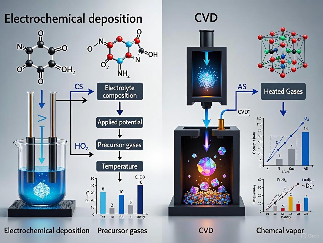
The synthesis of inorganic crystals and functional thin films is a cornerstone of modern materials science, with broad applications in electronics, energy storage, catalysis, and protective coatings. Two dominant methodologies for producing these materials are solution-phase electrochemical reduction (electrodeposition) and vapor-phase chemical reactions, most notably Chemical Vapor Deposition (CVD). These techniques operate on fundamentally different principles, involving distinct process mechanisms, experimental parameters, and resulting material properties.
Electrochemical reduction occurs in a liquid electrolyte, where dissolved metal ions are reduced on a substrate surface to form coatings or crystals. In contrast, vapor-phase CVD involves the thermal decomposition of gaseous precursor molecules on a heated substrate, leading to film growth. This guide provides a systematic comparison of these two foundational processes, highlighting their mechanisms, performance characteristics, and ideal application spaces to inform selection for specific research and development goals.
Fundamental Mechanisms and Pathways
The core distinction between these techniques lies in their reaction environments and the fundamental physics governing the deposition process.
Solution-Phase Electrochemical Reduction
This process is an electrically driven reaction occurring at the interface between a solid electrode and a liquid electrolyte. The key steps, as exemplified by Ni-Al₂O₃ composite coating deposition, include [1]:
- Mass Transport: Dissolved metal ions (e.g., Ni²⁺) and additive particles (e.g., Al₂O₃) are transported to the cathode surface through agitation and diffusion.
- Electron Transfer: Upon reaching the cathode, metal ions gain electrons and are reduced to their metallic state (e.g., Ni²⁺ + 2e⁻ → Ni⁰).
- Nucleation and Growth: Reduced atoms form nucleation sites, which grow into a crystalline or amorphous coating. Co-deposition of inert particles like Al₂O₃ can create composite coatings with enhanced properties [1].
Vapor-Phase Chemical Reactions (CVD)
CVD is a thermally driven process where film growth occurs from the gas phase. The fundamental steps, as illustrated in Figure 1(a) of the search results, involve [2]:
- Precursor Delivery and Gas Phase Reactions: Gaseous precursors are transported into a reaction chamber and may undergo homogenous gas-phase reactions.
- Surface Adsorption and Diffusion: Precursor molecules adsorb onto the heated substrate surface and diffuse across it.
- Heterogeneous Reaction and Nucleation: The adsorbed species undergo thermal decomposition or reaction with other gases, forming solid nuclei on the substrate.
- Film Growth: Nuclei grow through the continued incorporation of reaction products, forming a dense film [2].
The workflow diagrams below contrast the sequential steps of these two fundamental deposition mechanisms.
Figure 1: Experimental workflow for solution-phase electrochemical reduction (electrodeposition), illustrating the sequence from substrate preparation to film growth [1].
Figure 2: Experimental workflow for a typical vapor-phase Chemical Vapor Deposition (CVD) process, showing the path from precursor preparation to film growth [2].
Performance Comparison and Experimental Data
The fundamental differences in mechanism lead to distinct performance outcomes, which can be quantified through key metrics such as deposition rate, microstructure control, and material properties.
Quantitative Performance Comparison
Table 1: Comparative performance metrics for electrodeposition and CVD processes.
| Performance Metric | Solution-Phase Electrodeposition | Vapor-Phase CVD |
|---|---|---|
| Typical Deposition Rate | High (e.g., ~µm/min for Ni-Al₂O₃) [1] | Low to Medium [2] |
| Process Temperature | Near ambient (e.g., Room Temp - 80°C) [1] | High (e.g., 200°C > 1000°C) [2] |
| Microstructure Control | Good control over grain size and texture via current density and chemistry [1] | Excellent control over crystallinity, density, and phase via temperature and pressure [2] |
| Film Conformality | Poor on complex geometries | Excellent, uniform coverage on complex 3D structures [2] |
| Typical Film Density | Moderate, can be porous | Very high, pinhole-free [2] |
| Coating Composition | Pure metals, alloys, composites (e.g., Ni-Al₂O₃) [1] | Pure elements, ceramics, nitrides, carbides, complex functional oxides [2] |
| Energy Consumption | Primarily electrical energy for reduction | Primarily thermal energy for precursor decomposition and substrate heating [2] |
Impact of Process Parameters on Material Properties
Experimental data demonstrates how process inputs determine final material characteristics. In electrodeposition, the current density and bath chemistry critically determine the texture orientation and microstructure of the resulting coatings [1]. For instance, the concentration of boric acid in a Watts-type nickel plating bath can shift the preferential crystal orientation from (200) to (220), directly influencing hardness and wear resistance [1].
In CVD, the substrate temperature and precursor chemistry are paramount. Recent advances show that applying external electric or magnetic fields during CVD can exert additional control at the microscale, enabling low-temperature deposition, selected area deposition, and directional grain growth, thus transcending restrictions imposed by macroscopic parameters alone [2].
Experimental Protocols
This section outlines standard experimental methodologies for both techniques, providing a foundational protocol for researchers.
Table 2: Key reagent solutions for Ni-Al₂O₃ composite electrodeposition.
| Reagent Solution | Function in the Process |
|---|---|
| Watts Bath Electrolyte (Nickel Sulfate, Nickel Chloride, Boric Acid) | Provides Ni²⁺ ions for reduction; chloride minimizes anode passivation; boric acid acts as a pH buffer. |
| Al₂O₃ Powder (α-phase) | Reinforcement particles to form a composite coating, enhancing hardness and wear resistance. |
| Acetone | Solvent for degreasing and cleaning the substrate before deposition to ensure good adhesion. |
| Hydrochloric Acid (HCl) Pickling Solution | Removes surface oxides and impurities from the substrate prior to electrodeposition. |
- Substrate Preparation: Use medium carbon steel discs. Embed in phenolic resin to define a working surface area. Polish to a mirror finish. Clean and degrease by immersion in acetone, followed by rinsing with distilled water. Perform acid pickling in 50 g/L HCl solution at 40°C for one minute to remove surface oxides, then rinse and dry.
- Electrolyte Preparation: Prepare a standard Watts bath electrolyte containing nickel sulfate (240-320 g/L), nickel chloride (45-60 g/L), and boric acid (30-40 g/L). Add α-Al₂O₃ powder (10-25 g/L) as the reinforcement phase. Use magnetic stirring (e.g., 600 rpm for 16 hours) to ensure a homogeneous suspension.
- Electrodeposition Setup: Use a high-purity nickel plate as the soluble anode. Connect the prepared substrate as the cathode. Maintain a set distance (e.g., 2 cm) between the electrodes.
- Process Execution: Deposit using direct current (DC). Key parameters to control and optimize include:
- Current density: 2-5 A/dm²
- Agitation rate: 200-350 rpm
- Deposition time: 15-60 minutes
- Bath temperature: 40-60°C
- Post-Processing: After deposition, rinse the coated substrate with distilled water and dry. Characterization of coating properties can include microhardness testing, scanning electron microscopy (SEM) for morphology, energy-dispersive spectroscopy (EDS) for composition, and X-ray diffraction (XRD) for crystallinity.
- Substrate Preparation and Loading: The substrate (e.g., silicon wafer) is meticulously cleaned using standard procedures (e.g., RCA clean) to remove organic and ionic contaminants. It is then loaded into the CVD reactor chamber.
- Reactor Evacuation and Heating: The reactor chamber is evacuated to a base pressure and purged with an inert gas. The substrate is heated to the desired deposition temperature using resistive heating (hot-wall CVD) or by heating only the substrate holder (cold-wall CVD).
- Precursor Delivery and Deposition: The precursor(s) are delivered into the chamber. This may involve:
- Bubbling: An inert carrier gas (e.g., Ar, N₂) is bubbled through a liquid precursor to transport its vapor.
- Direct Flow: For gaseous precursors (e.g., SiH₄, CH₄).
- The precursor flow rates, chamber pressure, and substrate temperature are maintained for a set duration to achieve the target film thickness.
- Chamber Purge and Cool Down: After the deposition cycle, precursor flows are stopped, and the chamber is purged with inert gas to remove any unreacted precursors and byproducts. The substrate is then cooled to room temperature under vacuum or inert atmosphere before being unloaded.
The Scientist's Toolkit: Essential Research Reagents and Materials
Selecting the correct precursors and reagents is critical for successfully executing either deposition technique and achieving the desired material properties.
Table 3: Essential materials and their functions for electrodeposition and CVD processes.
| Material / Reagent | Function / Role | Example Use Case |
|---|---|---|
| Metal Salts (e.g., NiSO₄) | Source of metal ions (Mⁿ⁺) for reduction at the cathode. | Electrodeposition of pure Ni and Ni-composite coatings [1]. |
| Soluble Anode (e.g., Ni plate) | Replenishes metal ions in the solution and maintains electrical circuit. | Prevents depletion of Ni²⁺ ions in a Watts bath during DC electrodeposition [1]. |
| Boric Acid (H₃BO₃) | pH buffer agent in the electrolyte. | Maintains stable pH at the cathode-solution interface during nickel electrodeposition [1]. |
| Reinforcement Particles (e.g., Al₂O₃, YSZ) | Second-phase particles to form composite coatings. | Co-deposited with Ni to enhance microhardness and wear resistance [1]. |
| Volatile Precursors (e.g., Metalorganics, Halides) | Source of material to be deposited in gaseous form. | TiCl₄ and CH₄ are used in the CVD of TiC coatings [2]. |
| Carrier Gas (e.g., Ar, N₂, H₂) | Transports precursor vapors into the reaction chamber; can be reactive (H₂) or inert (Ar). | Hydrogen can act as a reducing agent in the CVD of metals from their halides [2]. |
| Reactive Gases (e.g., O₂, NH₃, CH₄) | React with precursor vapors to form the desired solid phase (oxide, nitride, carbide). | Oxygen is used for growing SiO₂ from SiH₄; ammonia for forming BN from BF₃ [2]. |
Solution-phase electrochemical reduction and vapor-phase CVD offer distinct pathways for materials synthesis, each with its own strengths and ideal applications.
Solution-Phase Electrodeposition is highly suited for depositing thick, metallic coatings and composites on simpler geometries where its cost-effectiveness, high deposition rates, and ability to form metal-matrix composites are major advantages. Its limitations typically lie in lower throwing power for complex shapes and generally less-precise microstructural control compared to CVD.
Vapor-Phase CVD excels in applications demanding high-purity, dense, and conformal films with superior control over crystallinity, stoichiometry, and microstructure. It is the preferred method for coating complex 3D structures and for depositing a vast range of non-metallic materials, including ceramics and semiconductors. The primary trade-offs often involve higher operational temperatures, more complex equipment, and the need for volatile precursors.
The choice between these two fundamental process mechanisms ultimately depends on the specific material system, the required film properties, the substrate limitations, and the economic constraints of the intended application. Advances in both fields, such as pulsed electrodeposition for grain refinement and field-enhanced CVD for low-temperature processing, continue to push the boundaries of their capabilities.
The pursuit of advanced materials in modern technology is fundamentally rooted in the precise control of thin film synthesis. Nucleation and growth kinetics represent a critical domain of study, dictating the structural, morphological, and functional properties of coatings and layers used across industries from microelectronics to energy storage. Two dominant methodologies—electrochemical deposition (ECD) and chemical vapor deposition (CVD)—offer distinct pathways for material fabrication, each governed by unique mechanisms and kinetic principles [3]. This guide provides an objective, data-driven comparison of these techniques, focusing on their application in growing inorganic crystals and thin films. It synthesizes current research to equip scientists and engineers with the necessary insights for selecting and optimizing deposition processes for specific research and development goals, framed within a broader thesis on inorganic materials synthesis.
Fundamental Principles and Kinetic Frameworks
Electrochemical Deposition (ECD) Kinetics
Electrochemical deposition is a solution-based process where ions in an electrolyte are reduced on a conductive substrate to form a solid phase. The kinetics are primarily driven by applied potential and are often described by classical nucleation theory (CNT).
- Nucleation Mechanism: The process initiates with the formation of stable atomic clusters, overcoming a free energy barrier. The free energy of formation for a cluster of size n is given by ΔGf,n = ΔG0n + kbTχn2/3, where the surface energy term creates an energetic barrier [4]. The critical nucleus size, beyond which growth becomes favorable, is defined by this maximum.
- Growth Dynamics: Following nucleation, growth proceeds via kinetically controlled or diffusion-controlled pathways, significantly influencing the final microstructure [5]. The growth rate and morphology can be tailored by parameters such as overpotential, ion concentration, and electrolyte pH [6].
- Site Selectivity: A key characteristic of ECD is its propensity for preferential nucleation at edge planes and surface defects. Studies on CVD-grown monolayer graphene show that MoO2 nanowires selectively nucleate at edge plane sites, affirming their higher electrochemical reactivity compared to the basal plane [7].
Chemical Vapor Deposition (CVD) Kinetics
Chemical vapor deposition involves the thermal decomposition and reaction of gaseous precursors on a heated substrate, resulting in the formation of a solid film.
- Nucleation Mechanism: In contrast to ECD, CVD nucleation involves precursor adsorption, surface diffusion, and decomposition [8]. The growth is typically atom-by-atom or molecule-by-molecule, with the growth plane often determined by the surface nucleation stage with the lowest energy [9].
- Energetics and Activation: Traditional CVD relies on high temperatures (600–800°C) to drive precursor decomposition. However, Plasma-Enhanced CVD (PECVD) utilizes a high-energy stream of ionized molecules to lower the required substrate temperature to a range of 200–400°C, enabling deposition on temperature-sensitive materials [10].
- Morphological Control: The growth of specific crystal structures, such as two-dimensional inorganic molecular crystals (2DIMCs), can be challenging due to weak crystalline anisotropy. Innovative approaches like Passivator-Assisted Vapor Deposition (PAVD) use passivators to suppress low-energy planes and promote lateral, two-dimensional growth [9].
The following diagram illustrates the fundamental pathways from initial precursor/ion to final film structure for both ECD and CVD.
Comparative Performance Analysis
The choice between ECD and CVD significantly impacts the properties and performance of the resulting materials. The following tables provide a quantitative and qualitative comparison based on experimental data.
Table 1: Fundamental Characteristics and Process Conditions
| Feature | Electrochemical Deposition (ECD) | Chemical Vapor Deposition (CVD) |
|---|---|---|
| Primary Driving Force | Applied electrical potential [11] [6] | Thermal energy (precursor decomposition) [8] [10] |
| Process Medium | Liquid electrolyte (aqueous/organic) [3] [6] | Vapor/gas phase [8] [9] |
| Typical Operating Temperature | Near room temperature to 90°C [11] | Thermal CVD: 600–800°CPECVD: 200–400°CPIB-CVD: Room Temperature [10] |
| Deposition Rate | High, tunable via current density | Variable, depends on precursor flux and temperature |
| Key Controlled Parameters | Potential/current, electrolyte composition, pH [6] | Temperature, pressure, precursor gas flow rate [8] |
| Energy Consumption Profile | Lower thermal energy, electrical energy for ion reduction | High thermal energy for precursor cracking and substrate heating |
Table 2: Quantitative Performance Metrics for Specific Material Systems
| Material / Application | Method | Key Performance Metrics & Findings | Reference |
|---|---|---|---|
| Silicon-based Anodes for Li-ion batteries | ECD vs. CVD | ECD: Simple, flexible, low-cost, long cycle life. CVD: High-quality, uniform films, but often requires higher temperatures. | [3] |
| ZnO Nanowires | ECD | Growth on Graphene/Cu: Smaller diameter nanowires, stronger photoluminescence emission compared to growth on bare Cu. | [11] |
| 2D Sb₂O₃ Molecular Crystals | PAVD (CVD variant) | Achieved monolayer thickness (~0.64 nm), lateral size >20 µm. Passivator enables 2D growth by suppressing low-energy planes. | [9] |
| Copper/Copper Oxide Composites | ECD | Formation of Cu₂O crystals possible by controlling overpotential and local pH. Crystal shape and geometry tunable via deposition time. | [6] |
| Diamond Coatings on WC-Co tools | CVD (with ECD pretreatment) | ECD Pretreatment: Selective Co removal (from 6.1% to 0.3%), surface polishing. CVD: Subsequent high-quality, adherent diamond coating. | [12] |
Experimental Protocols and Methodologies
Protocol for Electrochemical Deposition of ZnO Nanowires
This protocol, adapted from the synthesis of ZnO nanowires on CVD-graphene/Cu electrodes, highlights a typical ECD workflow for growing functional metal oxide nanostructures [11].
- Electrolyte Preparation: Prepare an aqueous solution of 100 mM Zn(NO₃)₂·6H₂O and 100 mM KNO₃. KNO₃ acts as a supporting electrolyte to enhance conductivity.
- Substrate Preparation: Use a conductive substrate such as a Cu foil or a Cu foil coated with CVD-grown graphene. Clean the substrate thoroughly with solvents (e.g., acetone, isopropanol) and dry.
- Electrochemical Setup: Employ a standard three-electrode system.
- Working Electrode: The prepared substrate (Cu or G/Cu).
- Counter Electrode: A Pt mesh.
- Reference Electrode: A saturated calomel electrode (SCE) or Ag/AgCl.
- Deposition Parameters: Maintain the electrolyte temperature at 90°C. Apply a constant cathodic potential between -0.8 V and -1.2 V (vs. Ref.) for a defined period (e.g., 30-60 minutes) without stirring.
- Post-Deposition Handling: After deposition, rinse the sample thoroughly with distilled water to remove residual salts and dry in air or under a nitrogen stream.
Protocol for Passivator-Assisted CVD of 2D Sb₂O₃ Crystals
This protocol details the synthesis of two-dimensional inorganic molecular crystals, showcasing a advanced CVD approach [9].
- Setup Configuration: Use a three-zone tube furnace. Place atomically flat mica substrates in the downstream region of the quartz tube.
- Precursor and Passivator Loading:
- Route 1 (InCl₃ assisted): Place hydrophilic SbCl₃·xH₂O precursor in the upstream zone and InCl₃ passivator in a separate boat in the central zone.
- Route 2 (Se assisted): Use Se powder as the passivator instead of InCl₃.
- Gas Environment and Heating: Evacuate the tube and maintain a constant argon flow. Heat the precursor zone to 320°C to generate SbOCl vapor. Simultaneously, heat the substrate zone to 400°C.
- Reaction and Growth: The vapors (SbOCl, H₂O, and passivator) are transported to the hot substrate zone where they react to form Sb₂O₃ flakes. The passivator critically suppresses heterophase nucleation and promotes lateral growth.
- Termination and Characterization: After a growth period (e.g., 30 minutes), cool the furnace to room temperature under argon flow. The resulting ultrathin flakes can be characterized by AFM, Raman spectroscopy, and SEM.
The workflow below visualizes the key stages of a generalized CVD process, including the crucial role of a passivator.
The Scientist's Toolkit: Essential Research Reagents and Materials
Successful deposition requires careful selection of precursors, substrates, and other reagents. The following table outlines key materials used in the featured ECD and CVD experiments.
Table 3: Essential Research Reagents and Materials
| Item | Function / Role | Example Application |
|---|---|---|
| Zn(NO₃)₂·6H₂O | Source of Zn²⁺ ions in the electrolyte for ECD. | Electrochemical deposition of ZnO nanowires [11]. |
| KNO₃ | Supporting electrolyte; increases conductivity without participating in the reaction. | Electrochemical deposition of ZnO nanowires [11]. |
| Copper(II) Sulphate (CuSO₄) | Source of Cu²⁺ ions for electrodeposition of copper and its oxides. | Formation of Cu/Cu₂O nanocomposite coatings [6]. |
| SbCl₃·xH₂O | Vapor-phase precursor supplying SbOCl for Sb₂O₃ formation. | PAVD growth of 2D Sb₂O₃ molecular crystals [9]. |
| InCl₃ / Se Powder | Passivator agent; controls nucleation plane and suppresses 3D growth in CVD. | PAVD growth of 2D Sb₂O₃ molecular crystals [9]. |
| Methane (CH₄) | Carbon source gas for CVD growth of graphene. | CVD synthesis of graphene on Cu substrates [11]. |
| CVD-Graphene/Cu | Conductive substrate with modified surface properties. | Provides a surface for controlled nucleation and growth of ZnO nanowires via ECD [11]. |
| Cemented Carbide (WC-Co) | Substrate for hard coatings. Requires pretreatment for CVD. | Substrate for CVD diamond coatings after ECD cobalt removal [12]. |
Application-Specific Performance and Selection Guidelines
The optimal deposition technique is largely determined by the target application, as each method offers distinct advantages for specific material properties and performance requirements.
Energy Storage Materials (e.g., Li-ion Battery Anodes): For silicon-based anodes, ECD is valued for its simplicity, low cost, and ability to produce films with a long cycle life [3]. It allows for the creation of nanostructured and composite films that can accommodate volume changes during lithiation. Conversely, CVD can produce high-purity, uniform silicon thin films, though often at a higher cost and temperature.
Wear-Resistant and Hard Coatings: CVD is the dominant technique for applying ultra-hard coatings like diamond. A key challenge is the detrimental effect of cobalt in WC-Co substrates. Here, ECD pretreatment proves highly effective by selectively etching surface cobalt, creating an ideal surface for subsequent high-quality, adherent CVD diamond growth [12].
Electronic and Optoelectronic Devices: CVD is unparalleled for producing high-quality, large-area semiconductor films, such as graphene and 2D molecular crystals [9] [7]. ECD finds a complementary role in the functionalization of these materials; for instance, by selectively depositing metal oxides like MoO₂ onto the edge planes of graphene to create nanowires or modify electronic properties [7].
Low-Temperature and Sensitive Substrate Processing: When deposition on plastics, pre-fabricated electronics, or other temperature-sensitive materials is required, low-temperature ECD and plasma-enhanced CVD (PECVD or PIB-CVD) are the primary options. PIB-CVD, in particular, offers room-temperature deposition with high tunability of film properties, making it suitable for flexible electronics and display manufacturing [10].
The synthesis of inorganic crystals is a cornerstone of modern materials science, underpinning advancements in fields ranging from electronics to drug delivery. The properties of these crystals—and their subsequent applications—are intrinsically governed by the methods used to create them. Among the myriad of synthesis techniques, chemical vapor deposition (CVD) and electrochemical deposition (ED) represent two pivotal approaches with distinct philosophies towards energy input and the subsequent activation of chemical reactions. This guide provides an objective comparison of these techniques, focusing on how thermal, plasma, and electrical energy inputs direct reaction pathways and influence the characteristics of the resulting inorganic crystals. Framed within contemporary materials research, which increasingly leverages artificial intelligence and autonomous experimentation for synthesis optimization [13] [14], this comparison aims to equip researchers with the data needed to select and optimize the appropriate synthesis method for their specific application.
Fundamental Principles and Energy Coupling Mechanisms
The primary distinction between CVD and ED lies in their phase transition pathways and how energy is coupled into the system to drive reactions.
Chemical Vapor Deposition (CVD) is a process where solid material is deposited onto a substrate through the vapor-phase chemical reaction of precursors [2]. In thermal CVD, the necessary activation energy for precursor decomposition and surface reactions is supplied entirely as heat, often requiring high temperatures (several hundred to over a thousand degrees Celsius) [2]. This thermal energy overcomes the activation barriers for gas-phase and surface reactions. In plasma-enhanced CVD (PECVD), a non-thermal plasma provides an alternative energy pathway. Here, energetic electrons within the plasma generate highly reactive species (ions, radicals, and excited molecules) through electron-impact collisions, enabling these reactions to proceed at significantly lower substrate temperatures [2] [15].
Electrochemical Deposition (ED) is a solution-based process where electrical energy directly drives the reduction of metal ions at a cathode (substrate), leading to the formation of a solid crystalline film [16]. The key controlled parameter is the applied current or potential, which governs the reduction rate and supersaturation level of metal hydroxides or metals at the electrode-solution interface, thereby controlling nucleation and growth [16].
Table 1: Comparison of Fundamental Reaction Mechanisms and States of Matter.
| Feature | Chemical Vapor Deposition (CVD) | Electrochemical Deposition (ED) |
|---|---|---|
| Primary Energy Input | Thermal, Photonic, or Plasma (Electrical) | Electrical (Potential/Current) |
| Reaction Phase | Vapor-Phase to Solid-Phase | Liquid-Phase (Solution) to Solid-Phase |
| Core Mechanism | Chemical decomposition/reaction of precursors on a heated substrate or via plasma activation. | Electrochemical reduction of metal ions at a cathode. |
| Key Controlled Parameters | Substrate temperature, pressure, precursor gas flow rates, plasma power. | Applied current density/potential, electrolyte concentration, temperature, pH. |
| Typical By-products | Gaseous reaction products (e.g., H₂, HCl, CO₂). | Molecular Hydrogen (H₂), pH changes in electrolyte. |
Comparative Analysis of Synthesis Outcomes and Performance
The different energy input mechanisms of CVD and ED directly translate to variations in the capabilities, performance, and resulting material properties of each technique.
Process Capabilities and Material Characteristics
CVD is renowned for producing high-purity, dense, and conformal thin films with excellent adhesion on complex geometries [2]. It is the industry standard for applications requiring extreme fidelity, such as semiconductor devices and high-performance coatings. The use of plasma enhancement (PECVD) extends these benefits to temperature-sensitive substrates like polymers [2] [15]. In contrast, ED excels in its relatively low energy consumption, operational simplicity, and suitability for continuous production [16]. It is particularly effective for producing high-purity crystals and is easily scalable. However, its product morphology can be sensitive to electrolyte composition and local pH changes at the electrode [16].
Quantitative Performance Data
The following table summarizes key performance metrics and experimental parameters for the two techniques, drawing from specific experimental studies on magnesium hydroxide ED and general CVD processes.
Table 2: Experimental Parameters and Synthesis Outcomes for Inorganic Crystal Growth.
| Parameter / Outcome | Electrochemical Deposition (for Mg(OH)₂) | Chemical Vapor Deposition (General) |
|---|---|---|
| Temperature | Near-ambient (e.g., 30-70°C) [16] | Several hundred °C (Thermal CVD); Near-ambient to ~300°C (PECVD) [2] [15] |
| Energy Input Control | Current Density (e.g., 1.25 - 5.00 mA/cm²) [16] | Substrate Temperature, Plasma Power |
| Key Precursor/Electrolyte | Mg²⁺ concentration (e.g., 0.05-0.20 mol/L) [16] | Metal-organic or halide precursors in vapor phase [2] |
| Growth Rate | Highly dependent on current density and ion concentration [16] | Governed by temperature and precursor flux [2] |
| Process Pressure | Atmospheric | Sub-atmospheric to Atmospheric [2] |
| Crystal Quality / Purity | High product purity [16] | High purity, dense, conformal films [2] |
| Notable Findings | Nucleation rate increases exponentially with current density; Growth rate peaks at intermediate Mg²⁺ concentration [16]. | Plasma allows low-temp deposition; External fields (E/M) can control texture and density [2]. |
Experimental Protocols for Technique-Specific Synthesis
Protocol: Electrochemical Deposition of Mg(OH)₂ Crystals
This protocol is adapted from the study on understanding the nucleation and growth of magnesium hydroxide [16].
1. Materials and Setup:
- Electrolyte: Aqueous solution of MgCl₂·6H₂O (e.g., 0.10 mol/L).
- Electrodes: A suitable cathode (e.g., platinum or stainless steel) and an inert anode.
- Cell: A three-electrode electrolysis cell equipped with a real-time microzone pH sensor near the cathode surface.
- Instrumentation: Potentiostat/Galvanostat for precise current control.
2. Experimental Procedure:
- Prepare the MgCl₂ electrolyte solution in deionized water.
- Place the cathode and anode in the solution, ensuring the pH sensor is positioned in the cathode microzone.
- Set the bath temperature to a specific value (e.g., 50°C) using a thermostat.
- Apply a constant current density (e.g., 2.5 mA/cm²) across the electrodes.
- Monitor the pH change in the cathode microzone in real-time; a sharp increase signifies the onset of OH⁻ generation and the nucleation induction period.
- Continue the deposition for a set duration to achieve the desired crystal thickness.
- Remove the cathode, rinse with deionized water, and dry to obtain the Mg(OH)₂ crystals.
3. Data Analysis:
- The nucleation induction period (t_ind) is determined as the time between applying the current and the observed sharp inflection in the microzone pH [16].
- Nucleation and growth rates are calculated based on ex-situ characterization of the crystals (e.g., using microscopy) correlated with the applied current density and ion concentration.
Protocol: Plasma-Enhanced Chemical Vapor Deposition (PECVD)
This protocol outlines a generalized PECVD process for thin-film deposition, as reviewed in recent literature [2].
1. Materials and Setup:
- Precursors: Volatile precursor gases or vapors (e.g., metalorganics, SiH₄).
- Substrate: Properly cleaned substrate (e.g., silicon wafer, glass).
- Reactor: A vacuum-compatible PECVD reactor chamber (e.g., Dielectric Barrier Discharge - DBD type).
- Gas System: Mass flow controllers for precise delivery of precursor and carrier gases.
- Plasma Source: RF or microwave power source with matching network.
2. Experimental Procedure:
- Load the substrate into the reactor and evacuate the chamber to a base pressure.
- Introduce the precursor and carrier gases (e.g., Ar, H₂) at controlled flow rates to achieve the desired working pressure.
- If required, heat the substrate to a moderate temperature (e.g., 100-300°C).
- Ignite the plasma by applying RF/microwave power at a defined density.
- Maintain the deposition for a set time to achieve the target film thickness.
- Terminate the plasma power, stop the precursor flow, and allow the system to cool under an inert gas atmosphere.
- Remove the deposited sample for characterization.
3. Data Analysis:
- Film properties are characterized using techniques like spectroscopic ellipsometry (thickness), X-ray diffraction (crystallinity), and scanning electron microscopy (morphology and conformity).
Reaction Pathways and Workflow Visualization
The distinct reaction pathways for ED and PECVD are visualized below, highlighting the sequence of events from energy input to crystal formation.
Diagram 1: A comparison of the primary reaction pathways in Electrochemical Deposition (top, red) and Plasma-Enhanced CVD (bottom, blue). Each pathway begins with an electrical energy input but proceeds through fundamentally different physical and chemical steps to form the final inorganic crystal film.
The workflow for modern materials discovery, which often involves autonomous optimization of these techniques, is illustrated below.
Diagram 2: The closed-loop workflow for autonomous experimentation (Self-Driving Labs) applied to materials synthesis. This AI-driven approach iteratively designs, executes, and analyzes experiments to rapidly optimize synthesis parameters or test hypotheses for both CVD and ED processes [13].
The Scientist's Toolkit: Essential Research Reagents and Materials
This section details key reagents and materials essential for conducting experiments in electrochemical deposition and chemical vapor deposition.
Table 3: Key Research Reagents and Materials for CVD and Electrochemical Deposition.
| Item Name | Function / Application | Technical Specification / Notes |
|---|---|---|
| Metalorganic Precursors | Source of metallic element in CVD. Volatile compounds transported in vapor phase. | e.g., Trimethylaluminum (TMA) for Al, Tetraethylorthosilicate (TEOS) for Si. High purity required [2]. |
| MgCl₂·6H₂O | Source of Mg²⁺ ions in the electrochemical deposition of magnesium hydroxide. | Analytical grade. Concentration in electrolyte directly influences supersaturation and growth kinetics [16]. |
| Inert Carrier Gas | Transport medium for vapor precursors in CVD. | e.g., High-purity Argon (Ar) or Nitrogen (N₂). Flow rate is a critical process parameter [2]. |
| Potentiostat/Galvanostat | Instrument for controlling current or potential in electrochemical deposition. | Must provide stable, precise control of current density, a key variable governing nucleation rates [16]. |
| Microzone pH Sensor | In-situ monitoring of local pH changes near the cathode during electrochemical deposition. | Crucial for real-time determination of the nucleation induction period [16]. |
| Dielectric Barrier Discharge (DBD) Reactor | Generating non-thermal plasma for PECVD. | Allows low-temperature deposition on sensitive substrates. Configuration impacts plasma-catalyst contact [2] [17]. |
The selection of appropriate synthesis techniques is fundamental to advancing materials science, as the method of fabrication directly dictates a material's fundamental properties and its suitability for advanced applications. Among the plethora of available techniques, electrochemical deposition (ECD) and chemical vapor deposition (CVD) have emerged as two of the most pivotal and widely adopted methods for creating thin films, coatings, and complex material architectures. ECD, a solution-based process, leverages electrical currents to reduce metal ions from an electrolyte onto a conductive substrate, enabling the formation of metallic and composite coatings at relatively low temperatures [18]. In contrast, CVD involves the vapor-phase transport and reaction of precursor molecules on a heated substrate, resulting in the deposition of high-purity, dense films of metals, semiconductors, nitrides, and complex oxides [2] [19]. The intrinsic characteristics of these processes—including their underlying mechanisms, operational parameters, and material compatibility—make them uniquely suited for specific material classes and end-use applications.
This guide provides an objective, data-driven comparison of ECD and CVD, focusing on their application across key material systems from elemental metals to complex oxides and nitrides. By synthesizing current experimental data and detailing standard research protocols, this analysis aims to equip researchers and development professionals with the necessary insights to select the optimal deposition technique for their specific material challenges, particularly within the context of electrochemical and inorganic crystals research.
Comparative Analysis: Electrochemical Deposition vs. Chemical Vapor Deposition
The following section provides a direct, data-supported comparison of the core characteristics, performance, and material outputs of ECD and CVD processes.
Table 1: Core Characteristics and Process Parameters
| Feature | Electrochemical Deposition (ECD) | Chemical Vapor Deposition (CVD) |
|---|---|---|
| Basic Principle | Electrochemical reduction of ions from a solution onto a conductive substrate [18]. | Vapor-phase chemical reactions of precursors on a heated substrate [2]. |
| Typical Materials | Elemental metals (e.g., Cu), Alloys, Metal oxides (e.g., Cu₂O), Composites (e.g., Metal/CNT) [18]. | Nitrides (e.g., TiCN), Oxides, Elemental semiconductors, 2D materials (e.g., Graphene), Complex oxides [2] [19] [20]. |
| Standard Temperature | Near ambient to moderate (e.g., room temperature to ~90°C) [18]. | High temperature (e.g., 300°C to 1000°C+) [2] [19]. |
| Key Parameters | Applied voltage/current, electrolyte composition/pH, deposition time [18]. | Substrate temperature, precursor chemistry & flow rate, chamber pressure [2]. |
| Growth Rate | High (can exceed 1 µm/min) [18]. | Low to Moderate (nm to µm per hour) [2]. |
| Film Conformality | Varies; can be excellent on complex geometries. | Excellent, providing uniform and conformal coatings [2]. |
| Vacuum Required | No | Yes (for most variants) |
| Relative Cost | Lower | Higher |
Table 2: Performance and Material Properties of Representative Coatings
| Material System | Deposition Technique | Key Experimental Conditions | Resulting Properties / Performance |
|---|---|---|---|
| Copper / Cu₂O Crystals [18] | ECD | Solution: 1-100 mM CuSO₄, Voltage: 7.0 V, Substrate: CNT-coated stainless steel | Formation of various crystal forms; Raman spectroscopy identified pure Cu and Cu(I) oxide (Cu₂O) crystals. |
| TiCN Coatings [19] | CVD | Temp: ~1000°C, Precursor: TiO₂ & C powder, Reactive gas: N₂ | Hardness: ~28 GPa; Roughness: Increased from 40.88 nm to 48.25 nm with N₂ flow; Superior corrosion resistance vs. uncoated substrate. |
| Graphene Electrodes [20] | CVD | Temp: 1000°C, Precursors: CH₄ & H₂ gas, Substrate: Cu foil | High conductivity; uniform 2D structure; used as a base electrode for biomolecule immobilization. |
| CNT Conductive Coatings [21] | EPD (a type of ECD) | Voltage: 40 V, Time: 30-90 s, Suspension: CNTs in isopropanol | Resistance dropped to as low as 0.2 kΩ; homogeneous and compact CNT coatings on polymer mats. |
Experimental Protocols for Key Studies
To ensure reproducibility and provide a clear framework for researchers, this section outlines the detailed methodologies from several seminal studies cited in the comparison tables.
Protocol 1: Electrochemical Deposition of Copper/Copper(I) Oxide Nanocomposites
This protocol, adapted from a 2023 study, details the formation of nanocomposites composed of carbon nanotubes (CNTs) and copper-based crystals on a stainless steel substrate [18].
- Substrate Preparation: Austenitic chromium-nickel steel (AISI 304) plates are mechanically ground and ultrasonically cleaned in acetone and ethanol [18].
- CNT Functionalization: Multi-walled CNTs are chemically oxidized in a 3:1 (v/v) mixture of sulfuric acid (H₂SO₄) and nitric acid (HNO₃) at 70°C for 4 hours to introduce negatively charged carboxyl groups [18].
- Electrophoretic Deposition (EPD) of CNTs:
- Dispersion Preparation: Oxidized CNTs are dispersed in a 2:1:1 (v/v/v) mixture of acetone, ethanol, and distilled water at a concentration of 1 mg/mL, followed by sonication for 5 minutes [18].
- Process: The stainless steel substrate (anode) is placed between two counter electrodes (cathodes). A constant voltage of 30 V is applied for 60 seconds to deposit a layer of CNTs. The sample is then dried at room temperature [18].
- Electrochemical Deposition (ECD) of Copper Species:
- Electrolyte Preparation: An aqueous solution of copper(II) sulphate (CuSO₄) is prepared. Concentrations of 1 mM and 100 mM are used to vary crystal morphology [18].
- Process: The CNT-coated substrate acts as the cathode. Electrochemical deposition is performed at a constant voltage of 7.0 V for durations ranging from 60 to 600 seconds [18].
- Characterization: The resulting samples are characterized using Scanning Electron Microscopy (SEM), Electron Dispersive Spectroscopy (EDS), Raman spectroscopy, and Grazing Incidence X-ray Diffraction (GIXD) to analyze morphology, composition, and crystal structure [18].
Protocol 2: CVD of TiCN Hard Coatings
This protocol describes the synthesis of titanium carbonitride (TiCN) coatings at high temperature via CVD, as reported in a 2020 study [19].
- Substrate Preparation: A p-type c-Si (100) substrate is meticulously cleaned using the standard RCA (Radio Corporation of America) cleaning technique to remove organic and metallic contaminants [19].
- Precursor Loading: Titanium dioxide (TiO₂) and carbon (C) base powders are mixed in a 1:1 ratio and placed in a ceramic boat, which is then positioned in the heating zone of a horizontal CVD chamber. The silicon substrate is placed adjacent to the powder mixture [19].
- CVD Process:
- The chamber is sealed, and the temperature is raised to a constant, high value (specific to the reactor).
- Nitrogen (N₂) gas is introduced into the chamber as the reactive gas. The flow rate of N₂ is a critical parameter, with variations (e.g., 50, 100, 150 sccm) used to control coating properties [19].
- The deposition is carried out for a fixed duration at the target temperature [19].
- Post-Processing & Characterization: After deposition, the coated substrates are analyzed for surface morphology (SEM, AFM), microstructure (XRD), electrochemical corrosion resistance, and nanomechanical properties (nanoindentation for hardness) [19].
Protocol 3: CVD of Monolayer Graphene and Electrode Fabrication
This protocol covers the growth and transfer of high-quality graphene for electrochemical applications [20].
- Substrate Preparation: A copper foil (30 µm thick) is cleaned with ultrasonic waves in DI water, ethanol, and acetone [20].
- CVD Growth:
- PMMA-Assisted Graphene Transfer:
- A layer of Poly-methyl methacrylate (PMMA) is spin-coated onto the graphene/copper foil [20].
- The underlying copper is etched away by floating the sample on a 0.5 M Fe(NO₃)₃ solution [20].
- The PMMA/graphene layer is rinsed in DI water and transferred onto a target substrate (e.g., SiO₂/Si) [20].
- The PMMA is finally dissolved by immersing the sample in acetone overnight [20].
- Electrode Fabrication: Electrical contacts are formed by thermally evaporating nickel (10 nm) and gold (50 nm) layers onto the edge of the transferred graphene film [20].
Workflow Visualization
The following diagram illustrates the logical progression and key decision points in selecting and applying ECD and CVD for different material systems, based on the experimental data.
The Scientist's Toolkit: Essential Research Reagents & Materials
Successful execution of ECD and CVD research relies on a suite of high-purity reagents and materials. The following table details key items and their functions as derived from the cited experimental protocols.
Table 3: Essential Research Reagents and Materials
| Item | Function / Application | Example from Research |
|---|---|---|
| Copper(II) Sulphate (CuSO₄) | Source of Cu²⁺ ions for electrochemical deposition of copper and copper oxide crystals [18]. | Used in 1 mM and 100 mM concentrations to control crystal formation during ECD [18]. |
| Carbon Nanotubes (CNTs) | Used as a conductive scaffold or reinforcing phase in composite coatings; can be deposited via EPD [18] [21]. | Electrophoretically deposited on stainless steel before Cu ECD [18]. |
| High-Purity Acids (H₂SO₄, HNO₃) | Chemical functionalization of nanomaterials (e.g., CNTs) to introduce surface charge for dispersion and deposition [18]. | Used in a 3:1 mixture for oxidizing CNTs to enable EPD [18]. |
| Methane (CH₄) & Hydrogen (H₂) | Common precursor and carrier/reducing gas in CVD for growing carbon-based nanomaterials and thin films [2] [20]. | Used as carbon source and reducing atmosphere in graphene CVD growth [20]. |
| Titanium Dioxide (TiO₂) & Carbon Powder | Solid precursors for CVD of titanium carbide (TiC) and titanium carbonitride (TiCN) coatings [19]. | Mixed in a 1:1 ratio and used with N₂ gas to deposit TiCN coatings [19]. |
| Nitrogen (N₂) Gas | Reactive gas for introducing nitrogen into coatings during CVD, forming nitride phases [19]. | Flow rate varied (50-150 sccm) to control properties of TiCN coatings [19]. |
| Poly-methyl methacrylate (PMMA) | Polymer support layer for the transfer of delicate 2D materials (e.g., graphene) from growth substrates to target substrates [20]. | Used as a support to transfer CVD graphene from Cu foil to SiO₂/Si [20]. |
| Ultra-Pure Inorganic Reagents | Foundational for reproducible synthesis and device performance; impurities can skew results and compromise performance in electronics and catalysis [22]. | Critical for cleaner electronics fabrication and reliable trace analysis [22]. |
Technique Implementation and Target Applications in Advanced Technology
In the fields of materials science and engineering, controlled deposition of thin films and coatings is a cornerstone for advancing technology in sectors ranging from electronics to biomedical devices. Two of the most pivotal techniques in this domain are electrodeposition (ED) and chemical vapor deposition (CVD), which differ fundamentally in their approach, operating conditions, and application landscapes. Electrodeposition operates through an electrochemical reaction in a liquid electrolyte, allowing for the controlled deposition of metal ions onto a conductive substrate. In contrast, chemical vapor deposition occurs in a gaseous environment within a vacuum chamber, where precursor gases undergo thermal decomposition to form solid coatings on substrates. This guide provides a detailed, objective comparison of these two methodologies, framing them within the broader context of inorganic crystals research for electrochemical and materials applications. By examining their respective experimental setups, performance characteristics, and optimization strategies, this analysis aims to equip researchers and development professionals with the data necessary to select the appropriate technique for their specific application requirements.
The comparative analysis presented herein is particularly relevant for applications requiring precise control over material properties, including wear resistance, corrosion protection, and tailored electrochemical activity. Recent advances in both techniques have been accelerated by the integration of autonomous experimentation and AI-driven optimization, which allows for more rapid exploration of parameter spaces and deeper scientific understanding of deposition phenomena. As the demand for advanced functional materials grows, understanding the capabilities and limitations of these deposition technologies becomes increasingly critical for innovation across scientific and industrial domains.
Fundamental Process Principles
Electrodeposition (ED), also referred to as electroplating, is an electrochemical process where metal ions in an electrolyte solution are reduced and deposited onto a conductive substrate through the application of an electric current. The process requires an anode (source of metal ions), a cathode (substrate to be coated), and an electrolyte solution containing dissolved metal salts. When current flows, oxidation occurs at the anode, releasing metal ions into the solution, while reduction at the cathode causes metal ions to deposit as a solid film. This process allows for good control over coating thickness and composition through manipulation of current density, temperature, and electrolyte chemistry. Electrodeposition is particularly valued for its ability to coat complex geometries with uniform layers and its compatibility with a wide range of metals and alloys.
Chemical Vapor Deposition (CVD) describes a family of processes where a substrate is exposed to volatile precursor gases that decompose and react on the substrate surface to produce a desired deposit. CVD processes occur in vacuum chambers where precise control of gas composition, flow rates, temperature, and pressure enables the growth of high-purity, high-performance solid materials. Unlike electrodeposition, CVD does not require electrically conductive substrates and can deposit a wider variety of materials, including ceramics, semiconductors, and diamond films. Hot-filament CVD (HFCVD), a common variant, uses heated filaments to crack precursor gases, facilitating diamond growth on various substrates. The complex interplay of transport phenomena and reaction kinetics in CVD allows for exquisite control over film microstructure and properties, albeit with typically higher equipment and operational costs than electrodeposition.
Direct Performance Comparison
Table 1: Direct comparison of key characteristics between electrodeposition and chemical vapor deposition
| Characteristic | Electrodeposition | Chemical Vapor Deposition |
|---|---|---|
| Process Mechanism | Electrochemical reduction in liquid electrolyte [23] [24] | Thermal decomposition in vapor phase [13] [25] |
| Typical Operating Environment | Aqueous electrolyte solution at ambient pressure | Vacuum chamber at controlled pressure and temperature |
| Typical Coating Materials | Metals (Ni, Cu, Zn, Cr) and alloys [24] [1] | Diamond, ceramics, semiconductors, specialized alloys [13] [25] |
| Adhesion Strength | Moderate metallic bonding [23] [24] | Strong molecular bonding [23] |
| Wear Resistance | Moderate [23] [24] | Excellent [23] |
| Corrosion Resistance | Good (depends on metal type) [23] [24] | Superior [23] |
| Environmental Impact | Chemical waste requiring disposal [23] [24] | Environmentally friendly, no toxic byproducts [23] |
| Coating Uniformity on Complex Shapes | Excellent throwing power | Line-of-sight limitations, may require rotation |
| Typical Deposition Rate | 0.1-10 μm/min | 0.001-0.1 μm/min |
| Relative Cost | Low to moderate [24] | High [23] [24] |
| Heat Resistance | Limited; may degrade under heat [23] | Excellent; maintains integrity at high temperatures [23] |
Advanced Process Variations
Both electrodeposition and CVD have evolved beyond their basic implementations to include specialized techniques that expand their capabilities. Advanced electrodeposition methods include pulse electrodeposition and composite co-deposition. Pulse electrodeposition uses modulated current to achieve better grain structure control and more uniform deposits, particularly in high-aspect-ratio features. Composite co-deposition, as demonstrated in Ni-Al₂O₃ systems, suspends ceramic nanoparticles in the electrolyte that become incorporated into the growing metal matrix, significantly enhancing hardness and wear resistance [1]. These composite coatings can achieve microhardness improvements exceeding 160% compared to pure metal deposits [1].
CVD technology similarly encompasses numerous specialized approaches. Hot-filament CVD (HFCVD) is particularly important for diamond film synthesis, using strategically positioned filaments to crack precursor gases at temperatures exceeding 2000°C while maintaining substrates at lower temperatures [25]. Other variants include plasma-enhanced CVD (PECVD) that lowers deposition temperatures enabling coating of temperature-sensitive materials, and atomic layer deposition (ALD) which provides exceptional thickness control at the atomic scale through self-limiting surface reactions. The emergence of autonomous experimentation (AE) systems for CVD represents a particularly significant advancement, combining artificial intelligence with robotics to design, execute, and analyze deposition experiments in rapid, iterative cycles [13]. These self-driving labs can optimize synthesis parameters and test scientific hypotheses more efficiently than human researchers alone, accelerating materials discovery and process optimization.
Experimental Setups and Methodologies
Standard Electrodeposition Setup for Composite Coatings
The electrodeposition of nickel-alumina (Ni-Al₂O₃) composite coatings represents a well-established methodology for enhancing surface properties of components. The following protocol outlines a standardized approach optimized using Taguchi methods [1]:
Apparatus and Reagents:
- Electrolyte Cell: 200 mL Pyrex glass beaker
- Power Supply: Direct current (DC) source with adjustable current density (2-5 A·dm⁻²)
- Anode: High-purity nickel plate (99.8%) as soluble anode
- Cathode/Substrate: Medium carbon steel discs (20 mm diameter × 4 mm thickness)
- Electrolyte Composition: Watts bath containing nickel sulfate (240-300 g·L⁻¹), nickel chloride (45-90 g·L⁻¹), boric acid (30-45 g·L⁻¹)
- Reinforcement Phase: Aluminum oxide (Al₂O₃) powder (10-25 g·L⁻¹) with particle size typically 0.1-1.0 μm
- Agitation System: Magnetic stirrer with controlled rotation speed (200-350 rpm)
Substrate Preparation:
- Section substrates to required dimensions using a precision cutting instrument.
- Mount specimens in phenolic resin using a hot mounting press to define a consistent working surface area of 3.14 cm².
- Polish mounted substrates to a mirror finish using progressively finer abrasives.
- Clean and degrease by immersion in acetone for 1 minute followed by rinsing with distilled water.
- Etch in hydrochloric acid solution (50 g·L⁻¹) at 40°C for 1 minute to remove surface oxides.
- Rinse again with distilled water and dry thoroughly before deposition.
Deposition Procedure:
- Prepare electrolyte by dissolving Watts bath components in distilled water.
- Add Al₂O₃ powder to the electrolyte and stir continuously at 600 rpm for 16 hours to ensure homogeneous suspension.
- Position anode and cathode parallel to each other with an inter-electrode distance of 2 cm.
- Immerse electrodes in the electrolyte maintained at constant temperature (typically 45-55°C).
- Apply DC current at predetermined density (2-5 A·dm⁻²) for specified duration (15-60 minutes).
- Maintain constant agitation (200-350 rpm) throughout deposition to ensure uniform particle distribution.
- Remove coated substrate, rinse with distilled water, and dry for characterization.
Table 2: Optimization parameters for Ni-Al₂O₃ composite electrodeposition [1]
| Parameter | Level 1 | Level 2 | Level 3 | Level 4 | Optimal Value |
|---|---|---|---|---|---|
| Current Density (A·dm⁻²) | 2 | 3 | 4 | 5 | 4 |
| Al₂O₃ Concentration (g·L⁻¹) | 10 | 15 | 20 | 25 | 20 |
| Deposition Time (min) | 15 | 30 | 45 | 60 | 60 |
| Agitation Rate (rpm) | 200 | 250 | 300 | 350 | 300 |
Hot-Filament CVD Setup for Diamond Electrodes
The deposition of boron-doped diamond (BDD) electrodes via hot-filament CVD represents a sophisticated application of vapor deposition for advanced electrochemical applications. The following protocol details the fabrication of ceramic-based BDD electrodes [25]:
Apparatus and Reagents:
- Reactor Chamber: Custom-built HFCVD system with vacuum capability
- Filament Material: Tungium or rhenium wires arranged in parallel arrays
- Substrate: Kaolinite-cordierite ceramic (5 cm × 5 cm × 0.25 cm) with pre-drilled holes for electrical contacting
- Precursor Gases: Hydrogen (1000 mL·min⁻¹), methane (12 mL·min⁻¹), trimethylborate (0.15 mL·min⁻¹) as boron source
- Pressure Control System: Capable of maintaining 3.3 mbar operating pressure
- Temperature Monitoring: Optical pyrometry or thermocouple for substrate temperature measurement
Substrate Preparation:
- Subject ceramic substrates to particle blasting (SiC-F150, 4 bar) to enhance adhesion.
- Clean ultrasonically in ethanol to remove particulate contaminants.
- Seed with nano-diamond particles (1:500 in ethanol) using ultrasonic treatment to create nucleation sites.
- Dry seeded substrates in clean environment before loading into CVD reactor.
Deposition Procedure:
- Load prepared substrates between parallel filament arrays (30 mm spacing) in CVD chamber.
- Evacuate chamber to base pressure (typically <10⁻² mbar).
- Introduce hydrogen gas and activate filaments to operating temperature (approximately 2000°C).
- Heat substrates to deposition temperature of 850°C (±10°C) using filament radiation.
- Introduce methane and trimethylborate precursors into gas stream.
- Maintain deposition conditions for 42 hours to achieve approximately 7 μm coating thickness.
- Terminate gas flows and cool system under hydrogen atmosphere.
- Remove coated substrates for post-processing.
Post-Deposition Processing:
- Perform laser structuring using infrared laser (λ = 1064 nm, 100 W, 10 kHz) to create interdigitated electrode patterns.
- Set laser parameters to 60 mm/s scan speed with total structural path of 233.8 cm per sample side.
- Electrochemically anodize laser-structured regions at 10 V in distilled water for 2 minutes to remove sp² carbon residues.
- Characterize final electrode structure using SEM, Raman spectroscopy, and electrochemical testing.
Workflow Visualization
Diagram 1: Comparative workflow for electrodeposition and CVD processes
Research Reagent Solutions and Materials
Table 3: Essential research reagents and materials for deposition experiments
| Category | Specific Material/Reagent | Function/Purpose | Example Application |
|---|---|---|---|
| Electrodeposition Components | Nickel Sulfate (NiSO₄·6H₂O) | Primary source of nickel ions in Watts bath | Ni and Ni-Al₂O₃ coatings [1] |
| Nickel Chloride (NiCl₂·6H₂O) | Increases conductivity, prevents anode passivation | Ni and Ni-Al₂O₃ coatings [1] | |
| Boric Acid (H₃BO₃) | pH buffer, improves deposit quality | Watts bath formulations [1] | |
| Aluminum Oxide (Al₂O₃) Powder | Reinforcement phase for composite coatings | Wear-resistant Ni-Al₂O₃ composites [1] | |
| CVD Precursors | Hydrogen (H₂) | Carrier gas, removes non-diamond carbon | Diamond CVD [25] |
| Methane (CH₄) | Carbon source for diamond growth | Boron-doped diamond electrodes [25] | |
| Trimethylborate (B(OCH₃)₃) | Boron doping source for p-type semiconductor | Conductive diamond electrodes [25] | |
| Substrate Materials | Medium Carbon Steel | Conductive substrate for electrodeposition | Ni-Al₂O₃ composite coatings [1] |
| Kaolinite-Cordierite Ceramic | Thermally stable, electrically insulating substrate | Ceramic-based BDD electrodes [25] | |
| Silicon Wafers | Semiconductor substrate with well-defined surface | BDD on silicon for comparison [25] | |
| Preparation Materials | Nano-diamond Powder (50-100 nm) | Seeding material for diamond nucleation | Enhanced diamond growth on non-traditional substrates [25] |
| Silicon Carbide (SiC) Abrasive | Surface roughening for improved adhesion | Substrate preparation for ceramic BDD [25] | |
| Hydrochloric Acid (HCl) | Surface etching/activation | Substrate cleaning and oxide removal [1] |
Performance Data and Optimization Approaches
Quantitative Performance Metrics
Table 4: Experimentally measured performance outcomes for deposition processes
| Performance Metric | Electrodeposition Results | CVD Results | Testing Methodology |
|---|---|---|---|
| Coating Thickness | 5-50 μm (15-60 min deposition) [1] | ~7 μm (42 h deposition) [25] | Cross-sectional SEM, Laser microscopy |
| Microhardness | 164% increase for Ni-Al₂O₃ vs pure Ni [1] | >1.91 GPa for BDD [25] | Vickers micro-indentation |
| Al₂O₃ Incorporation | 400% increase at optimal parameters [1] | Not applicable | EDS elemental analysis |
| Crystallite Size | 20-60 nm (controlled by parameters) [1] | Microcrystalline facets >1 μm [25] | XRD Scherrer calculation, SEM |
| Energy Consumption | Lower operational energy | Higher (vacuum, high temperature) | 14-46% less for iDDE vs standard BDD [25] |
| Coating Adhesion | Moderate (metallic bonding) [24] | Excellent (molecular bonding) [23] | Tape test, scratch testing |
| Crystal Orientation | (220) preferential at high H₃BO₃ [1] | (111) orientation ratio up to 96% [26] | XRD texture analysis |
Process Optimization Methodologies
Both electrodeposition and CVD benefit significantly from systematic optimization approaches. The Taguchi method has been successfully applied to electrodeposition processes to identify critical parameters and their optimal ranges. Using an L₁₆ orthogonal array design, researchers can efficiently evaluate multiple factors simultaneously while minimizing experimental runs. For Ni-Al₂O₃ composite coatings, this approach has revealed that current density and deposition time exert the most significant influence on microhardness and particle incorporation, followed by alumina concentration and agitation rate [1]. The application of Analysis of Variance (ANOVA) further quantifies the relative contribution of each parameter to the observed results, enabling data-driven process optimization.
For CVD processes, autonomous experimentation (AE) systems represent the cutting edge in optimization methodology. These self-driving labs combine robotics, in situ characterization, and artificial intelligence to iteratively design and execute experiments without human intervention. The ARES CVD system developed by the Air Force Research Laboratory exemplifies this approach, using real-time Raman spectroscopy to characterize carbon nanotube growth and AI planners to select subsequent experimental conditions [13]. This closed-loop optimization can explore complex parameter spaces—including temperature, gas composition, and flow rates—more efficiently than traditional approaches, leading to both process optimization and fundamental scientific insights. For instance, AE campaigns have confirmed that CNT catalyst activity peaks when the metal catalyst is in equilibrium with its oxide, demonstrating how optimization can yield mechanistic understanding [13].
Diagram 2: Optimization methodologies for deposition processes
Application-Specific Implementation Guidance
Technology Selection Framework
Choosing between electrodeposition and chemical vapor deposition requires careful consideration of application requirements, material constraints, and economic factors. The following decision framework provides guidance for technology selection:
Select electrodeposition when:
- Applications require moderate wear and corrosion protection rather than extreme performance [23] [24]
- Cost sensitivity is a primary concern, particularly for high-volume production [24]
- Components have complex geometries requiring uniform coverage in recessed areas [24]
- Electrical conductivity is the primary functional requirement [24]
- Substrate materials are thermally sensitive and cannot withstand high temperatures [23]
- Rapid prototyping or benchtop-scale development is needed with limited capital investment
Select chemical vapor deposition when:
- Applications demand exceptional hardness, wear resistance, or durability [23]
- High-temperature performance is required for the coated component [23]
- Superior adhesion is critical for component lifetime and reliability [23]
- Complex material compositions (ceramics, diamonds, specialized semiconductors) are needed [13] [25]
- Environmental considerations favor processes without hazardous chemical waste [23]
- Applications require precise control over crystallinity and microstructure at the nanoscale
Emerging Applications and Future Directions
Recent advances in both electrodeposition and CVD have opened new application frontiers that leverage their respective capabilities. In electrochemical advanced oxidation processes (EAOPs) for water treatment, boron-doped diamond electrodes fabricated via CVD offer exceptional performance for degrading persistent organic pollutants [25]. The development of interdigitated double diamond electrodes (iDDE) with reduced interelectrode spacing (<50 μm) demonstrates how CVD-fabricated electrodes can achieve 14-46% energy savings compared to standard BDD technology, addressing both performance and sustainability requirements [25].
For electrodeposition, the integration of nanoparticle reinforcements and optimized process parameters has enabled the fabrication of composite coatings with dramatically enhanced properties. The 400% increase in alumina incorporation and 164% improvement in microhardness demonstrated in optimized Ni-Al₂O₃ systems illustrates the potential for electrodeposition to meet demanding mechanical requirements [1]. The continued development of pulse and pulse-reverse electrodeposition techniques further expands the capability to control grain structure, residual stress, and composition distribution in electrodeposited coatings.
The convergence of both technologies with digitalization and automation represents perhaps the most significant future direction. Autonomous experimentation systems for CVD are already demonstrating the ability to optimize complex multi-parameter processes and test scientific hypotheses with minimal human intervention [13]. Similar approaches are being applied to electrodeposition, where machine learning algorithms can identify optimal parameter combinations from limited experimental data. These advancements suggest a future where deposition processes are increasingly optimized through computational and robotic approaches, accelerating both fundamental understanding and technology deployment across research and industrial sectors.
The relentless pursuit of miniaturization and enhanced performance in semiconductor devices places immense importance on advanced fabrication techniques. Thin-film deposition processes are fundamental to forming interconnects, diffusion barriers, and transistor gates, directly influencing device speed, power efficiency, and reliability. This guide provides an objective comparison between two pivotal deposition methods: electrochemical deposition (ECD) and chemical vapor deposition (CVD), within the context of inorganic crystal growth for microelectronics. Framed for researchers and scientists, this analysis presents experimental data, detailed protocols, and key reagents to inform material selection and process development for next-generation devices.
Electrochemical deposition (ECD) is a well-established technique where metal ions dissolved in an electrolyte solution are reduced and deposited onto a conductive substrate through an applied electric potential. It is widely utilized for its cost-effectiveness and high deposition rates, particularly in the formation of copper interconnects. [27]
Chemical vapor deposition (CVD) involves the dissociation of vapor-phase precursor chemicals on a heated substrate surface, resulting in the formation of a solid thin film. Variants such as Plasma-Enhanced CVD (PECVD) and Atomic Layer Deposition (ALD) offer enhanced control, enabling deposition at lower temperatures and with superior conformality for complex three-dimensional architectures. [27] [2]
Table 1: Comparative Analysis of ECD and CVD for Semiconductor Fabrication
| Feature | Electrochemical Deposition (ECD) | Chemical Vapor Deposition (CVD) |
|---|---|---|
| Fundamental Principle | Electrochemical reduction of metal ions from a solution. [27] | Chemical reaction of vapor-phase precursors on a heated substrate. [27] |
| Typical Materials | Copper (Cu), Nickel (Ni), Gold (Au) for interconnects. [27] | Tungsten (W), Silicon Dioxide (SiO₂), Silicon Nitride (Si₃N₄), High-k dielectrics (e.g., HfO₂). [27] [28] |
| Deposition Rate | High. [27] | Moderate to Low; ALD is very low but highly controlled. [27] |
| Film Uniformity & Conformality | Can suffer from non-uniformity and poor step coverage in high-aspect-ratio features. [27] | Excellent uniformity and conformality, especially in ALD and PECVD. [27] [2] |
| Typical Process Temperature | Low (Near room temperature to <100°C). [27] | High (300-1000°C); PECVD enables lower temperatures (150-400°C). [27] [2] |
| Precursor Requirements | Metal salts in aqueous or organic electrolytes. [27] | High-purity, volatile gases or vapors (e.g., SiH₄, WF₆). [27] |
| Capital & Operational Cost | Relatively low cost and operational simplicity. [27] | High cost due to complex reactor systems and expensive precursors. [27] |
| Key Limitations | Unstable deposition quality, inadequate film uniformity, and limited precision control at micro/nanoscale. [27] | High thermal budget for conventional CVD; precursor chemistry limitations. [27] |
| Primary Applications in ICs | On-chip copper interconnects, through-silicon vias (TSVs), packaging. [27] | Gate electrodes (e.g., W), gate dielectrics, diffusion barriers (e.g., SiN), pre-metal dielectrics. [27] [28] |
Experimental Performance Data
Interconnect Fabrication: ECD vs. CVD Copper
The formation of copper interconnects is a critical application where ECD and CVD are directly compared. Experimental data from the literature highlights a performance trade-off.
Table 2: Experimental Comparison of Copper Interconnect Deposition
| Parameter | Electrochemical Deposition (ECD) of Cu | CVD of Cu |
|---|---|---|
| Resistivity (μΩ·cm) | ~1.98 (bulk, after annealing) [27] | ~2.5 - 3.5 (as-deposited, highly dependent on impurities and morphology) [27] |
| Deposition Rate | ~500 nm/min (excellent for high-throughput manufacturing) [27] | ~50 nm/min (slower, can be a bottleneck) [27] |
| Step Coverage in High-Aspect-Ratio Trenches | Moderate to poor; requires sophisticated additives and pulse plating for void-free filling. [27] | Good inherent conformality; can achieve uniform coatings without voids. [27] |
| Adhesion to Diffusion Barrier (e.g., TaN) | Excellent when surface is properly seeded and pre-treated. [27] | Good, but highly dependent on the surface chemistry of the barrier layer. [27] |
| Process Complexity | Requires management of additive chemistry (accelerators, suppressors, levelers) in the bath. [27] | Requires precise control of precursor temperature, vapor pressure, and decomposition kinetics. [27] |
Summary: ECD is the dominant industrial process for copper interconnects due to its high deposition rate and lower cost, achieving low resistivity post-annealing. However, it requires complex chemical additives to achieve void-free "superfilling" of features. CVD copper offers superior conformality without additives but suffers from higher resistivity and lower deposition rates, limiting its widespread adoption for this specific application. [27]
Barrier and Gate Layer Fabrication: The CVD and ALD Advantage
For diffusion barriers and gate stacks, CVD and its derivative, ALD, are unambiguously superior due to their atomic-level control.
Diffusion Barriers: As device features shrink, preventing copper diffusion into the silicon substrate is critical. While ECD cannot deposit an effective barrier material, CVD and ALD excel at depositing conformal, pinhole-free barrier layers like silicon nitride (SiN) or tantalum nitride (TaN). Experimental studies show that PECVD SiN barriers as thin as 20nm can effectively block copper diffusion at backend-of-line (BEOL) processing temperatures. [27] [28]
Gate Stacks: The fabrication of transistor gates demands ultra-thin, uniform, and high-quality dielectric materials. ECD has no role in this domain. In contrast, ALD, a variant of CVD, is the industry standard for depositing high-k dielectric materials (e.g., HfO₂) in gate-all-around (GAA) transistors. ALD provides the atomic-scale fidelity required for sub-5nm technology nodes, enabling equivalent oxide thicknesses of less than 1nm with low leakage currents. [28] Research on all-2D material field-effect transistors (FETs) using CVD-grown molybdenum disulfide (MoS₂) with graphene contacts has demonstrated the viability of CVD for next-generation device architectures, achieving room-temperature mobilities of ~14.5 cm²/V·s. [29]
Detailed Experimental Protocols
Protocol for Electrochemical Deposition of Copper Interconnects
This protocol outlines the standard process for void-free copper filling of high-aspect-ratio trenches on a silicon wafer with a PVD-deposited Ta/TaN barrier and a Cu seed layer.
- Substrate Preparation: A 300mm p-type silicon wafer with patterned oxide trenches and a physical vapor deposition (PVD)-deposited Ta/TaN barrier layer (10nm) and a PVD Cu seed layer (50nm) is used. The wafer is cleaned in a dilute sulfuric acid solution (H₂SO₄:H₂O = 1:10 v/v) for 60 seconds to remove native oxides from the Cu seed layer, then rinsed with deionized water.
- Electrolyte Preparation: The deposition bath is prepared with 0.7M CuSO₄, 1.0M H₂SO₄, 50 ppm Cl⁻ (from HCl), and proprietary organic additives including a suppressor (polyethylene glycol), an accelerator (bis-(sodium-sulfopropyl)-disulfide), and a leveler (janus green b).
- Deposition Process: The wafer is mounted on a cathode and immersed in the electrolyte at 25°C. Deposition is performed using a periodic pulse reverse plating waveform:
- Forward Pulse: +10 mA/cm² for 50 ms (deposition).
- Reverse Pulse: -30 mA/cm² for 5 ms (dissolution).
- This cycle promotes bottom-up superfill by differentially affecting deposition rates at the trench bottom versus the sidewalls.
- Post-Deposition Treatment: The wafer is rinsed with deionized water and subjected to an annealing step at 150°C for 30 minutes in a N₂ atmosphere to recrystallize the copper, reduce grain boundary scattering, and lower resistivity. [27]
Protocol for CVD of a Tungsten Gate Electrode
This protocol describes a low-pressure CVD (LPCVD) process for depositing a tungsten (W) gate electrode via hydrogen reduction of tungsten hexafluoride.
- Substrate Preparation: A silicon wafer with an ALD-deposited high-k dielectric layer (e.g., HfO₂) is loaded into the LPCVD reactor. The chamber is evacuated to a base pressure of <10⁻⁶ Torr.
- Pre-Deposition Step: To ensure good adhesion and nucleation, a thin (~5nm) "nucleation layer" of tungsten is often deposited using a silane (SiH₄) reduction process: 2WF₆ + 3SiH₄ → 2W + 3SiF₄ + 6H₂. This step is performed at 300°C and 1 Torr.
- Bulk Deposition Process: The temperature is raised to 450°C. The main deposition is carried out using the hydrogen reduction reaction: WF₆ + 3H₂ → W + 6HF. Process conditions are:
- WF₆ flow rate: 50 sccm
- H₂ flow rate: 500 sccm
- Chamber Pressure: 2 Torr
- Deposition Time: 10 minutes (to achieve a target thickness of ~50nm)
- Post-Deposition Treatment: The chamber is purged with argon gas. The wafer is unloaded after cooling to below 100°C. Subsequent chemical-mechanical polishing (CMP) is used to planarize the tungsten film and define the final gate structure. [27] [28]
Workflow Visualization
The following diagram illustrates the key decision-making workflow for selecting between ECD and CVD based on the target application in semiconductor fabrication.
The Scientist's Toolkit: Key Research Reagents & Materials
Table 3: Essential Materials for ECD and CVD Research in Microelectronics
| Item | Function/Description | Typical Application |
|---|---|---|
| Copper Sulfate Pentahydrate (CuSO₄·5H₂O) | High-purity source of Cu²⁺ ions in the electrolyte for ECD. | Copper interconnect deposition. [27] |
| Tungsten Hexafluoride (WF₆) | A highly volatile and reactive precursor gas for CVD of tungsten metal. | Gate electrode formation, contacts, and interconnects. [27] [28] |
| Silane (SiH₄) | A pyrophoric gas used as a precursor for silicon-based films and as a reducing agent. | CVD of silicon nitride (with NH₃) or silicon dioxide; reduction of WF₆ for W nucleation. [27] |
| Organic Additives (Suppressors, Accelerators, Levelers) | Chemicals that modulate the deposition rate at different surface sites to enable superconformal, void-free filling. | Electrochemical deposition of copper in high-aspect-ratio features. [27] |
| Hafnium Precursors (e.g., HfCl₄, TEMAH) | Metal-organic or halide precursors used in ALD/CVD processes for high-k dielectric films. | Deposition of HfO₂ as the gate dielectric in advanced logic transistors. [28] |
| Tantalum Nitride (TaN) Target | A sputtering target used in PVD systems to deposit a thin, continuous diffusion barrier layer. | Creates a conductive barrier on which a Cu seed layer for ECD is deposited. [27] |
The long-term success of biomedical implants—from coronary stents to orthopedic prostheses—hinges on their seamless integration with the human body. This requires not only biocompatibility to avoid adverse immune reactions but also, increasingly, the capacity for active therapeutic delivery. Surface engineering through advanced coating technologies provides a powerful strategy to meet these demands, creating interfaces that modulate biological responses and enhance clinical outcomes [30] [31].
Among the myriad of coating techniques, Chemical Vapor Deposition (CVD) and Electrochemical Deposition (ECD) have emerged as particularly potent methods. CVD involves the vapor-phase deposition of solid thin films through chemical reactions of precursor gases on a substrate surface, enabling precise control over film properties [2]. Its variant, Plasma-Enhanced CVD (PECVD), utilizes plasma to facilitate these reactions at significantly lower temperatures, making it suitable for temperature-sensitive materials [32] [33]. In parallel, a novel approach termed Electrodeposition of Polymer Networks (EPoN) has recently been demonstrated, enabling the fabrication of conformal, functional ultrathin films on conductive substrates under mild solution conditions [34]. This review provides a comparative analysis of these advanced coating methodologies, evaluating their performance, applications, and suitability for next-generation biomedical implants.
Technology Comparison: Deposition Mechanisms and Characteristics
Chemical Vapor Deposition (CVD) and Plasma-Enhanced CVD (PECVD)
CVD is a versatile platform technology for depositing thin films and coatings of functional materials. The process involves several elementary steps: precursor flow into a reaction chamber, thermal or plasma-induced decomposition of these precursors, adsorption of reactive species onto the substrate surface, intermolecular reactions, cluster formation, and diffusion to form a solid film [2]. The fundamental parameters controlling the CVD process include substrate temperature, reactor pressure, precursor flux, and the chemical nature of the precursors and carrier gases [2].
PECVD represents a significant advancement that expands CVD's applicability to biomedical domains. By utilizing high-energy electrons in non-equilibrium plasma to excite precursor molecules to higher electronic and vibrational states, PECVD initiates bond dissociation and facilitates thin film deposition at substantially lower temperatures compared to conventional thermal CVD [2]. This low-temperature processing is crucial for coating temperature-sensitive polymer-based implants and for incorporating heat-labile bioactive molecules.
Table 1: Comparison of CVD Variants for Biomedical Applications
| CVD Variant | Activation Mechanism | Typical Deposition Temperature | Key Advantages | Biomedical Applications |
|---|---|---|---|---|
| Thermal CVD | Thermal energy | High (often >500°C) | High purity, dense films | Limited due to high temperature |
| Plasma-Enhanced CVD (PECVD) | Plasma-generated radicals, ions, electrons | Low (room temperature to ~400°C) | Lower temperature, enhanced adhesion, broader material compatibility | Diamond-like carbon (DLC) coatings, barrier layers [32] [33] |
| Metalorganic CVD (MOCVD) | Thermal or plasma | Moderate to high | Precise stoichiometry control, complex oxides | Emerging for perovskite-based bioelectronics [35] |
| Aerosol-Assisted CVD | Thermal | Variable | Broad precursor compatibility, non-volatile precursors | Potential for drug-loaded coatings |
Electrochemical Deposition (ECD) and Electrodeposition of Polymer Networks (EPoN)
Electrochemical deposition encompasses techniques where electrical fields facilitate the deposition of materials onto conductive substrates from solution-based precursors. A recent innovation in this domain is the Electrodeposition of Polymer Networks (EPoN), which enables fabricating conformal polymeric ultrathin films on conductive substrates with arbitrary shapes under mild solution conditions [34].
The EPoN mechanism utilizes a dual-functional macromolecular design where polymers are appended with electrochemically active crosslinkers as side groups. When an oxidative potential is applied to the substrate, these crosslinkers (such as phenol) generate radicals that couple to form oligomeric crosslinks, creating a polymer network that precipitates onto the electrode surface [34]. This deposition is self-limiting—the growing film eventually becomes insulating, stopping further deposition and enabling precise thickness control. This mechanism permits conformal coating of complex 3D architectures, a significant advantage for porous implant structures.
A particularly powerful iteration is "reactive EPoN," where the deposited polymer network retains chemical functionality for post-deposition modification. For instance, polyisoprene coatings containing alkene groups in each repeating unit can be subsequently functionalized via thiol-ene "click" chemistry to introduce specific biofunctional groups [34]. This modular approach separates the deposition process from functionalization, preserving bioactive molecule integrity during the electrochemical step.
Table 2: Performance Comparison of Coating Technologies for Biomedical Implants
| Performance Characteristic | CVD/PECVD | ECD/EPoN |
|---|---|---|
| Coating Conformality | Moderate to high (depends on technique) | Excellent (self-limiting mechanism) [34] |
| Deposition Temperature | Wide range (room temp to high temp) | Ambient conditions [34] |
| Coating Thickness Control | Excellent (nanometer to micrometer) | Excellent (typically 100s of nanometers) [34] |
| Incorporation of Bioactives | Challenging (high temp/vacuum environment) | Facile (post-deposition functionalization) [34] |
| Coating Density/Barrier Properties | Excellent (dense, pinhole-free) | Good (dependent on crosslink density) |
| Substrate Limitations | None (with appropriate surface preparation) | Requires electrically conductive surface [34] |
| Equipment Complexity/Cost | High (vacuum systems, plasma generation) | Moderate (electrochemical cells, potentiostat) |
| Scalability for Complex Geometries | Good (with specialized fixtures) | Excellent (natural affinity for conductive surfaces) |
Experimental Protocols and Performance Data
CVD/PECVD Protocol for Diamond-Like Carbon (DLC) with Interlayers
Experimental Protocol: A recent study demonstrated a multi-step PECVD process for depositing DLC coatings with various interlayers on AISI 420 stainless steel substrates (common for medical devices) [32]. The protocol involved:
- Substrate Preparation: Samples (20 × 20 × 2 mm) were ground with SiC abrasive papers up to grit size 2500 and mirror-polished with 0.1 μm diamond paste, achieving surface roughness of 2-5 nm.
- Interlayer Deposition:
- Plasma Nitriding: Performed for 240 min at 5 kW power and 500-600 V voltage using 75% N₂ and 25% H₂ gas mixture.
- ZrN Deposition: RF magnetron sputtering with 99.999% pure Zr target for 60 min, base pressure 2.8 × 10⁻³ mbar, power 185 W, with 10% N₂ and 30% Ar.
- TaN Deposition: RF magnetron sputtering with 99.999% pure Ta target for 60 min, base pressure 1.1 × 10⁻⁴ mbar, power 100 W at 350°C, with 10% N₂ and 30% Ar.
- DLC Deposition: All samples were coated via PECVD using 100% pure acetylene gas at 45 mTorr pressure, 120 W power, for 45 minutes.
Performance Data: The incorporation of interlayers significantly enhanced DLC coating performance [32]:
- Surface Roughness: TaN+DLC (3.31 nm) and ZrN+DLC (3.42 nm) showed dramatically smoother surfaces than PN+DLC (42.34 nm).
- Wear Resistance: TaN+DLC exhibited the lowest weight loss (8 mg) and wear rate (0.001901 mm³/N·m) in pin-on-disk tests (2 N load, 150 m sliding distance).
- Corrosion Resistance: Electrochemical impedance spectroscopy in 3.5% NaCl solution showed TaN+DLC had the highest corrosion resistance.
EPoN Protocol for Reactive Polymer Networks
Experimental Protocol: The EPoN process for creating functionalized polymeric coatings involves [34]:
- Polymer Synthesis: Modification of polyisoprene with a small fraction (<5 mol%) of phenol side groups as electrochemically active crosslinkers.
- Electrodeposition: Application of an anodic potential to an indium tin oxide (ITO) coated glass substrate immersed in a solution containing the reactive polymer.
- Network Formation: Oxidation of phenolate side groups generates phenoxy radicals that couple into dimers and further oligomerize, forming a crosslinked polymer network on the electrode surface.
- Self-Limiting Growth: Film growth ceases when the deposited layer becomes insulating and impermeable to polymeric precursors.
- Post-Deposition Functionalization: Reactive alkene groups in the polyisoprene network are modified via thiol-ene chemistry with functional thiols (e.g., fluorinated alkyl thiols).
Performance Characteristics:
- Thickness Control: Film thickness tunable in the 100s of nanometers range by varying phenol fraction and electrodeposition potential.
- Conformality: Excellent coverage on complex 3D and porous electrode architectures.
- Functionalization Versatility: The reactive handle allows incorporation of diverse bioactive ligands without compromising deposition efficiency.
The Scientist's Toolkit: Essential Research Reagents and Materials
Table 3: Essential Research Materials for Coating Development
| Material/Reagent | Function | Application Examples |
|---|---|---|
| Acetylene (C₂H₂) | Carbon precursor for DLC synthesis | PECVD of DLC coatings [32] |
| Tantalum/Zirconium Targets | Sputtering sources for interlayer deposition | TaN, ZrN interlayers for enhanced adhesion [32] |
| Phenol-Functionalized Polymers | Electrochemically crosslinkable macromers | EPoN deposition of reactive networks [34] |
| Thiol-Functionalized Bioactive Molecules | Post-deposition functionalization | Introducing specific bioactivity to coatings [34] |
| Silane Coupling Agents | Surface primers for improved adhesion | Promoting coating-substrate adhesion |
| Nitrogen/Argon Gases | Process gases for sputtering and plasma generation | Reactive atmosphere for nitride formation [32] |
| Boron-Containing Precursors | CVD precursors for h-BN coatings | Boron trioxide, borane-dimethylamine complexes [36] |
The choice between CVD/PECVD and ECD/EPoN technologies for biomedical implant coatings depends heavily on the specific application requirements:
CVD/PECVD is preferable when:
- Exceptional hardness, wear resistance, and barrier properties are paramount (e.g., orthopedic bearing surfaces)
- Dense, pinhole-free coatings are required for corrosion protection
- High-temperature stability is needed for sterilization or in-service conditions
- Non-conductive substrates must be coated
ECD/EPoN is advantageous for:
- Temperature-sensitive substrates or bioactive molecules
- Complex 3D geometries requiring uniform conformal coverage
- Applications demanding post-deposition functionalization with biological ligands
- Rapid prototyping and moderate-cost equipment requirements
Emerging hybrid approaches that combine the robustness of CVD with the biofunctionality of electrochemical methods represent the future of advanced biomedical coatings. These integrated systems could potentially leverage PVD/CVD for base barrier layers followed by ECD/EPoN for bioactive surface functionalization, offering synergistic benefits for next-generation intelligent implant technologies.
Electrochemical Deposition vs CVD for Inorganic Crystals
The synthesis of inorganic crystals for advanced applications in energy storage and conversion is a cornerstone of modern materials science. Electrochemical deposition (ECD) and chemical vapor deposition (CVD) represent two fundamentally different paradigms for creating functional inorganic layers and microstructures. ECD achieves material growth through electrically driven reduction-oxidation reactions in a liquid electrolyte, typically at near-ambient temperatures [37] [38]. In contrast, CVD relies on thermally driven chemical reactions of vapor-phase precursors on a substrate, often requiring significantly higher temperatures [2] [39]. This guide provides a systematic comparison of these techniques, focusing on their applications in manufacturing battery electrodes, catalysts, and photovoltaic components, to inform material selection and process development.
Performance Comparison
The choice between ECD and CVD involves critical trade-offs between process scalability, material quality, energy consumption, and cost. The table below summarizes their core performance characteristics across key metrics relevant to industrial application and research.
Table 1: Comprehensive Performance Comparison of ECD and CVD
| Performance Metric | Electrochemical Deposition (ECD) | Chemical Vapor Deposition (CVD) |
|---|---|---|
| Typical Operating Temperature | Room temperature to low temperatures (e.g., 25°C) [38] | High temperatures (e.g., 320°C to >1000°C) [2] [40] [39] |
| Growth Rate | Can be very high (microns per second in meniscus-guided methods) [37] | Variable; can be low to moderate |
| Energy Consumption | Lower (not limited by Carnot efficiency) [39] | Higher (energy-intensive, Carnot cycle-limited) [39] |
| Scalability & Throughput | Excellent; highly compatible with roll-to-roll and large-area manufacturing [37] | Moderate; batch processing is common, though some continuous variants exist |
| Capital & Operational Cost | Generally lower cost, uses less expensive equipment [37] | Generally higher cost due to high-temperature and vacuum systems |
| Microstructural Control | Good for nanoparticles and dense films; can achieve precise nanostructures like Pt nanoparticles [37] | Excellent for high-purity, uniform, large crystal structures with few defects [39] |
| Conformality on 3D Structures | Good, but can be limited by current distribution | Excellent for complex geometries and high-aspect-ratio structures [2] |
| Environmental Impact (CO2 Footprint) | Lower; C2CNT variant consumes CO2 as a feedstock [39] | High CO2 footprint, especially when using methane and other potent GHG precursors [39] |
| Precursor Utilization | High efficiency in meniscus-confined setups (e.g., ~100 μL per deposition) [37] | Can be inefficient, with significant precursor waste |
| Material Versatility | Metals, alloys, metal oxides (e.g., LTO, Pt), some composites [37] [38] | Extremely broad: metals, ceramics, semiconductors, carbon nanotubes (CNTs), graphene [2] [39] |
Application-Specific Analysis
Battery Electrode Fabrication
Fabricating high-performance battery electrodes demands techniques that balance material quality, throughput, and cost. ECD and CVD offer distinct pathways.
Electrochemical Deposition: ECD shines in its ability to directly deposit active electrode materials onto current collectors at near-ambient conditions. A prime example is the direct electrodeposition of Lithium Titanate (LTO) anodes from a propylene carbonate solution containing titanyl compounds [38]. This single-step process forms various LTO phases (Li4Ti5O12, Li2Ti3O7) at room temperature, simplifying manufacturing and reducing energy consumption compared to traditional high-temperature solid-state synthesis. ECD is also pivotal in forming artificial solid electrolyte interphases (Art-SEI) via electro-polymerization of electrolyte additives, which stabilizes lithium metal anodes [41].
Chemical Vapor Deposition: While not typically used for direct, massive electrode powder production, CVD is unparalleled in growing high-purity, conformal coatings and advanced materials like carbon nanotubes (CNTs). CNTs produced via CVD can be incorporated into composites to enhance the mechanical strength and electrical conductivity of electrodes [39]. However, traditional CVD is a significant CO2 emitter. An emerging alternative, C2CNT (CO2 to CNT) , is an electrochemical method that produces CNTs by molten carbonate electrolysis of CO2, combining the material advantages of CNTs with a negative carbon footprint process [39].
Table 2: Battery Electrode Fabrication: ECD vs. CVD
| Feature | Electrochemical Deposition (ECD) | Chemical Vapor Deposition (CVD) |
|---|---|---|
| Primary Role | Direct deposition of active materials (e.g., LTO), formation of Art-SEIs [41] [38] | Synthesis of conductive additives (e.g., CNTs), thin functional coatings [39] |
| Process Temperature | Low (Room temperature to moderate) [38] | High (Several hundred °C) [39] |
| Key Advantage | Low energy, single-step deposition, ambient conditions [38] | High material quality, excellent conductivity of products like CNTs [39] |
| Key Disadvantage | Limited to electroactive species in solution | High energy cost and CO2 footprint for conventional CVD [39] |
Catalysts and Photovoltaics
The deposition of catalytic layers and photovoltaic components often requires precise control over nanostructure and film uniformity.
Electrochemical Deposition: ECD is a powerful tool for synthesizing nanostructured catalysts, such as platinum nanoparticles (Pt NPs) for dye-sensitized solar cells (DSSCs). The horizontal-dipping electrodeposition method can produce high-performance Pt NP counter electrodes in a single, rapid step. This technique is not only cost-effective but also compatible with roll-to-roll production and flexible substrates, making it highly attractive for industrial scaling [37]. The ability to use water-based precursors further enhances its eco-friendly profile.
Chemical Vapor Deposition: CVD and its advanced variants are workhorses in semiconductor and photovoltaic industries. For perovskite solar cells (PSCs), vapor-phase deposition techniques enable the fabrication of high-quality, pinhole-free perovskite films with exceptional control over stoichiometry, thickness, and uniformity across large areas [40]. This leads to improved device reproducibility and performance. Furthermore, Field-Enhanced CVD—which incorporates external electric (EF) or magnetic fields (MF)—offers additional control over nucleation, grain growth, and texture, transcending the limitations of conventional thermal parameters [2].
Table 3: Catalyst and Photovoltaic Application: ECD vs. CVD
| Feature | Electrochemical Deposition (ECD) | Chemical Vapor Deposition (CVD) |
|---|---|---|
| Typical Output | Metal nanoparticle catalysts (e.g., Pt) [37] | High-quality semiconductor films (e.g., Perovskites), 2D materials [40] |
| Microstructural Control | Good control over nanoparticle size and distribution [37] | Superior control over film uniformity, crystallinity, and grain structure [2] [40] |
| Scalability | Excellent for roll-to-roll catalyst deposition [37] | Excellent for large-area, uniform semiconductor films [40] |
| Process Complexity | Relatively simple, solution-based | Complex, requires vapor precursor handling and high-temperature reaction chambers |
Experimental Protocols
Protocol 1: Horizontal-Dipping Electrodeposition of Platinum Nanoparticles
This protocol details a scalable method for depositing Pt catalyst nanoparticles for DSSCs [37].
Key Reagents and Functions:
- Potassium tetrachloroplatinate(II) (K₂PtCl₄): Platinum precursor salt.
- Fluorine-doped tin oxide (FTO) glass: Conductive substrate.
- Deionized water: Solvent for the precursor solution.
Procedure:
- Solution Preparation: Dissolve K₂PtCl₄ in deionized water to prepare a 10 mM precursor solution.
- Apparatus Setup: Use a custom horizontal-dipping apparatus consisting of a platinum sheet counter electrode and a linear stage to move the substrate horizontally.
- Meniscus Formation: Bring the glass bar (counter electrode) to approximately 500 μm from the FTO substrate surface. Deposit ~100 μL of the precursor solution between them to form a stable meniscus connecting the bar and the substrate.
- Electrodeposition: Apply a constant current density of -0.5 mA cm⁻² for 60 seconds while the linear stage moves the substrate at a controlled speed (e.g., 100 μm s⁻¹).
- Post-processing: After deposition, rinse the coated FTO substrate with deionized water and dry it at room temperature. The entire process is complete in minutes and requires no thermal sintering.
Protocol 2: Direct Electrodeposition of Lithium Titanate (LTO)
This protocol describes a novel method for depositing LTO anode active material directly from an organic electrolyte [38].
Key Reagents and Functions:
- Titanyl Perchlorate (TiO(ClO₄)₂) or Titanyl Sulfate (TiOSO₄): Source of TiO²⁺ ions.
- Lithium Perchlorate (LiClO₄): Supporting electrolyte and lithium source.
- Propylene Carbonate (PC): Aprotic organic solvent.
- Water Traces (50 mM): Source of OH⁻ ions via electroreduction.
Procedure:
- Electrolyte Preparation: Prepare the deposition electrolyte by dissolving LiClO₄ and a titanyl compound (e.g., TiO(ClO₄)₂) in propylene carbonate. Add a controlled amount of water (50 mM).
- Electrochemical Cell Setup: Use a standard three-electrode cell with a conductive substrate (e.g., Ni foil) as the working electrode, a Pt counter electrode, and a Li/Li⁺ reference electrode.
- Electrodeposition: Perform electrodeposition by sweeping the potential from open-circuit voltage to a final potential of 1.2 V (vs. Li/Li⁺) at a scan rate of 1 mV s⁻¹.
- Reaction Mechanism: The process involves electroreduction of water to OH⁻, which reacts with TiO²⁺ ions to form TiO(OH)₂/TiOOH intermediates. These then react with Li⁺ ions in the solution to form various lithium titanate phases (Li₄Ti₅O₁₂, Li₂Ti₃O₇) directly on the electrode.
- Post-processing: Wash the deposited electrode with pure propylene carbonate to remove residual salts and dry under vacuum.
The Scientist's Toolkit
Successful implementation of ECD and CVD requires specific reagents and precursors. The table below lists essential materials for the experimental protocols discussed.
Table 4: Essential Research Reagents and Materials
| Reagent/Material | Function/Application | Associated Technique |
|---|---|---|
| Potassium tetrachloroplatinate(II) (K₂PtCl₄) | Platinum metal precursor for catalyst deposition [37] | Electrochemical Deposition |
| Titanyl Perchlorate (TiO(ClO₄)₂) | Titanium precursor for direct LTO electrodeposition [38] | Electrochemical Deposition |
| Lithium Perchlorate (LiClO₄) | Lithium source and supporting electrolyte in organic media [38] | Electrochemical Deposition |
| Propylene Carbonate (PC) | Aprotic organic solvent for air-sensitive electrochemistry [38] | Electrochemical Deposition |
| Fluorine-doped tin oxide (FTO) glass | Transparent conductive oxide substrate for photoelectrodes [37] | Both ECD and CVD |
| Methane (CH₄) | Common carbon feedstock for CVD growth of CNTs and graphene [39] | Chemical Vapor Deposition |
| Metal Catalysts (Ni, Fe) | Nanoparticle catalysts to initiate CNT growth in CVD [39] | Chemical Vapor Deposition |
| Diallyldimethylammonium salts | Monomers for forming polymeric ionic liquids (PILs) as solid electrolytes [42] | Material Synthesis for Devices |
Electrochemical deposition and chemical vapor deposition are both indispensable tools in the materials scientist's arsenal, yet they serve different strategic purposes. Electrochemical deposition is the champion of scalability, cost-effectiveness, and energy efficiency, particularly for depositing metallic catalysts and, as emerging research shows, certain metal oxide electrode materials directly from solution at low temperatures. Its compatibility with roll-to-roll processes makes it a prime candidate for industrial-scale manufacturing of devices like DSSCs and next-generation batteries.
Conversely, chemical vapor deposition remains unmatched in its ability to produce high-purity, high-performance crystalline films and advanced nanomaterials like CNTs with exceptional control over structure and properties. It is the go-to technique for applications demanding the highest material quality, such as high-efficiency perovskite photovoltaics and advanced semiconductor devices. The emergence of hybrid and field-enhanced CVD methods, along with transformative electrochemical alternatives like C2CNT that utilize CO2 as a feedstock, continues to push the boundaries of what these techniques can achieve. The optimal choice is not a matter of which technique is superior, but which is most appropriate for the target material, application, and production context.
Overcoming Technical Challenges and Process Optimization Strategies
The advancement of functional materials for energy storage and electronic devices heavily relies on precision engineering of thin films and coatings. Within materials science, two deposition techniques stand out for fabricating such structures: Chemical Vapor Deposition (CVD) and Electrodeposition. The former is often hampered by its intrinsic requirement for high processing temperatures, while the latter grapples with complexities of electrolyte compatibility. This guide provides an objective comparison of these techniques, focusing on their core limitations, and presents experimental data and methodologies relevant to researchers developing next-generation electrochemical devices.
The drive for miniaturization and enhanced performance in devices like all-solid-state batteries (ASSBs) necessitates sophisticated control over inorganic crystal growth. CVD is a versatile technique for producing high-purity, functional thin films through the vapor-phase decomposition of chemical precursors onto a substrate [2]. In contrast, Electrodeposition is a solution-based process that uses electrical current to reduce metal ions from an electrolyte onto a conductive substrate, forming a coherent coating [43] [1]. The selection between these methods involves critical trade-offs centered on thermal budget and interfacial control, which directly impact the microstructure, scalability, and ultimate performance of the deposited material.
Core Principles and Intrinsic Limitations: A Comparative Analysis
A fundamental understanding of each technique's mechanics and inherent constraints is crucial for informed selection. The table below summarizes their core characteristics and primary limitations.
Table 1: Fundamental Comparison of CVD and Electrodeposition
| Aspect | Chemical Vapor Deposition (CVD) | Electrodeposition |
|---|---|---|
| Basic Principle | Vapor-phase precursor decomposition and chemical reaction on a heated substrate [2]. | Electrochemical reduction of dissolved metal ions onto a conductive cathode [43] [1]. |
| Primary Limitation | High Processing Temperatures | Electrolyte Compatibility & Formulation |
| Typical Thermal Range | Several hundred degrees Celsius; can be lower with advanced variants (e.g., PECVD) [2]. | Typically near room temperature. |
| Key Challenge | High temperatures can degrade temperature-sensitive substrates, induce unwanted interfacial reactions, and increase energy consumption [44] [45]. | Requires precise control of pH, composition, and potential to avoid parasitic reactions, control morphology, and ensure adhesion [43] [1]. |
| Impact on Materials | Can lead to detrimental space-charge layers, interdiffusion, and crack formation in solid-state battery assemblies during deposition [44] [45]. | Incorrect parameters lead to porous films, high surface roughness, or loosely attached deposits [43]. |
The High-Temperature Hurdle in CVD
Conventional CVD processes rely on thermal energy to break chemical bonds in precursor molecules. This high-energy requirement often necessitates substrate temperatures exceeding 500°C to achieve the necessary kinetics for precursor decomposition and crystalline film growth [2]. For applications like solid-state batteries, where materials are often integrated into multilayer stacks, such high temperatures are a significant drawback. They can cause interfacial degradation, including the formation of resistive layers and interdiffusion between adjacent materials, which severely compromises device performance [44] [45]. Furthermore, these temperatures preclude the use of many polymer or low-melting-point substrates, limiting application versatility and increasing energy costs.
The Compatibility Conundrum in Electrodeposition
Electrodeposition circumvents high-temperature issues but introduces a different set of challenges centered on the electrolyte solution. The properties of the final deposit—including its morphology, adhesion, composition, and crystal structure—are exquisitely sensitive to the electrolyte's makeup and electrochemical conditions. Key parameters requiring precise control include:
- Solution pH: Critically influences film morphology; for instance, in Cu₂Se deposition, a pH below 1.5 was essential for achieving compact, smooth films, while higher pH increased roughness [43].
- Applied Potential: Determines the phase and adhesion of the deposit. For Cu₂Se, potentials below -0.37 V vs Ag/AgCl resulted in loosely attached films, while the desired Cu₂Se phase was stabilized at more negative potentials [43].
- Additives and Particle Incorporation: For composite coatings, the incorporation of particles like Al₂O³ requires optimization of concentration, agitation, and current density to achieve uniform dispersion and desired properties [1].
Failure to precisely manage these factors can result in poor adhesion, non-uniform growth, and the inclusion of impurities.
Experimental Data and Performance Comparison
Direct experimental data from recent studies highlights the practical outcomes and trade-offs associated with each method. The following table synthesizes key performance metrics and optimized conditions for both techniques.
Table 2: Experimental Data and Optimized Performance from Recent Studies
| Deposition Technique | Material System | Key Optimized Parameters | Resulting Properties & Performance |
|---|---|---|---|
| Electrodeposition [43] | Cu₂Se Thin Films | Potential: Below -0.37 V vs Ag/AgClSolution pH: < 1.5 | Surface Roughness: ~130 nmFilm Thickness: Up to 12.5 µmCrystal Size: ~18.4 nm |
| Electrodeposition [1] | Ni-Al₂O₃ Composite | Current Density: 2-5 A/dm²Al₂O₃ Concentration: 10-25 g/LAgitation Rate: 200-350 rpm | Microhardness Increase: 164%Al₂O₃ Incorporation Increase: 400%Crystallite Size: Notably reduced |
| CVD [2] | Functional Thin Films | Use of external fields (Plasma, Electric, Magnetic) | Deposition Temperature: Significantly loweredGrain Growth & Texture: Enhanced controlFilm Density & Conformality: Improved |
The data demonstrates that electrodeposition can produce high-quality, thick films with fine nanocrystalline structures at near-ambient temperatures. The optimization of parameters like potential and pH is critical for achieving superior morphology and adhesion. In contrast, advancements in CVD, particularly through the application of external fields, are primarily focused on mitigating its core limitation—high temperature—while simultaneously gaining finer control over film microstructure.
Detailed Experimental Protocols
To ensure reproducibility and provide a clear technical roadmap, this section outlines standardized protocols derived from the cited research.
Objective: To deposit smooth, thick, and well-adhered Cu₂Se films on a conductive substrate.
- Substrate Preparation: Clean the conductive substrate (e.g., Mo, steel) sequentially with acetone, distilled water, and a pickling acid (e.g., HCl) to remove organic and inorganic contaminants. Rinse thoroughly and dry.
- Electrolyte Preparation: Prepare an acidic aqueous solution containing copper ions (e.g., from CuSO₄) and selenous acid (H₂SeO₃). Precisely adjust the pH of the solution to < 1.5 using a strong acid like H₂SO₄.
- Electrodeposition Setup: Use a standard three-electrode cell with the prepared substrate as the working electrode, a platinum or graphite sheet as the counter electrode, and an Ag/AgCl (sat. KCl) reference electrode.
- Deposition Process: De-aerate the electrolyte with an inert gas (e.g., N₂). Maintain the electrolyte temperature at a constant value (e.g., 25°C). Apply a constant potential (-0.37 V to -0.6 V vs. Ag/AgCl) using a potentiostat. The deposition time will determine the final film thickness.
- Post-Processing: After deposition, carefully remove the coated substrate, rinse with distilled water to remove residual electrolyte, and dry under a nitrogen stream.
Objective: To maximize microhardness and Al₂O₃ incorporation while minimizing crystallite size in a composite coating.
- Experimental Design: Employ the Taguchi Method with an L₁₆ orthogonal array to efficiently investigate four key factors, each at four levels:
- Current Density (A/dm²): 2, 3, 4, 5
- Al₂O₃ Concentration (g/L): 10, 15, 20, 25
- Deposition Time (min): 15, 30, 45, 60
- Agitation Rate (rpm): 200, 250, 300, 350
- Coating Synthesis: Use a standard Watts bath (NiSO₄, NiCl₂, H₃BO₃) as the electrolyte. Disperse Al₂O₃ powder uniformly via continuous magnetic stirring (e.g., 600 rpm for 16 hours). Use a medium carbon steel disc as the cathode and a pure nickel plate as the anode. Perform electrodeposition experiments according to the L₁₆ array under direct current (DC).
- Analysis & Optimization: Characterize the coatings for microhardness (Vickers indentation), Al₂O₃ incorporation (EDS), and crystallite size (XRD). Analyze the data using Analysis of Variance (ANOVA) and Signal-to-Noise (S/N) ratio to determine the parameter set that simultaneously optimizes all responses.
Workflow and Pathway Visualization
The following diagrams illustrate the logical decision-making process for selecting a deposition technique and the generalized experimental workflows for each.
Deposition Technique Selection Pathway
Generalized Experimental Workflows
The Scientist's Toolkit: Essential Research Reagents and Materials
Successful execution of these deposition techniques requires specific materials and reagents. The table below details the key items and their functions for the featured experiments.
Table 3: Essential Research Reagents and Materials
| Item | Function/Application | Example from Protocols |
|---|---|---|
| Ag/AgCl Reference Electrode | Provides a stable, known potential for controlled potentiostatic electrodeposition [43]. | Used to maintain deposition potential between -0.37V and -0.6V for Cu₂Se [43]. |
| Potentiostat/Galvanostat | Instrument to precisely control the electrical potential or current during electrodeposition [43] [1]. | Essential for all electrodeposition experiments. |
| Metal Salts (e.g., NiSO₄, CuSO₄) | Source of metal ions in the electrolyte for the electrodeposition process [1]. | Core component of the Watts bath for Ni coatings [1]. |
| H₃BO₃ (Boric Acid) | Acts as a buffering and complexing agent in the electrolyte, stabilizing pH and influencing deposit structure [1]. | Used in the Watts bath for Ni-Al₂O₃ deposition [1]. |
| Al₂O₃ Powder (Sub-micron) | Reinforcement particles to create composite coatings with enhanced mechanical properties [1]. | Co-deposited with nickel to increase microhardness by 164% [1]. |
| Acidic Solutions (e.g., H₂SO₄, HCl) | Used for substrate pickling (cleaning) and for adjusting the pH of the electrolyte [43] [1]. | Critical for achieving pH < 1.5 for smooth Cu₂Se films [43]. |
| Vacuum Chamber & Heated Substrate Holder | Core components of a CVD system to create a controlled environment and provide thermal energy [2]. | Necessary for precursor decomposition and film growth in CVD. |
| Volatile Precursors (e.g., Metalorganics) | Source materials in vapor form for the CVD reaction [2]. | Varies by target material (e.g., precursors for Li₇La₃Zr₂O₁₂) [44]. |
The choice between CVD and Electrodeposition is not a matter of identifying a superior technology, but of matching technique strengths to application demands while effectively managing their intrinsic limitations. CVD's primary challenge of high temperature is being actively mitigated through innovative approaches like field-enhanced methods, making it indispensable for applications requiring ultra-pure, conformal films on thermally robust substrates. Electrodeposition offers a low-energy, scalable alternative but demands rigorous optimization of electrolyte chemistry and electrical parameters to control film properties and ensure compatibility.
For researchers in fields like solid-state battery development, this trade-off is critical. The integration of a garnet-type solid electrolyte like LLZO might favor advanced CVD for its purity, whereas depositing a copper selenide thermoelectric layer might be more efficiently achieved through optimized electrodeposition. Future developments will likely focus on hybrid approaches and further refinement of these techniques to narrow their respective limitations, paving the way for more efficient and versatile materials fabrication.
This guide objectively compares two foundational techniques for depositing inorganic crystals and thin films: Electrochemical Deposition (ED) and Chemical Vapor Deposition (CVD). The comparison is framed within research on advanced materials for applications ranging from microelectronics to energy storage, providing researchers with a data-driven analysis of each method's performance.
The pursuit of advanced materials in semiconductors, energy storage, and protective coatings critically depends on depositing high-quality thin films. The controlled formation of inorganic crystals on a substrate is governed by techniques that manipulate precursor delivery, nucleation, and growth kinetics. Among the most prevalent are Electrochemical Deposition (ED) and Chemical Vapor Deposition (CVD), along with their advanced variants.
Electrochemical Deposition (ED) is a well-established technique where metal ions in a solution are electrochemically reduced and deposited onto a conductive cathodic surface. It is widely used for applications such as semiconductor packaging and interconnects. [27]
Chemical Vapor Deposition (CVD) relies on chemical reactions in the vapor phase to deposit solid thin films onto a substrate. The process involves feeding volatile precursors into a reactor, where they decompose and react on a heated substrate, forming a coherent film. [2] CVD encompasses numerous phenomenologically related processes, including:
- Plasma-Enhanced CVD (PECVD): Uses plasma to allow for lower-temperature deposition, critical for temperature-sensitive substrates and advanced semiconductor packaging. [2] [46]
- Initiated CVD (iCVD): A low-temperature, gas-phase polymerization technique for depositing uniform and conformal polymer thin films, even on porous structures. [47]
The following diagram illustrates the core operational principles and logical relationship between these two fundamental techniques.
Direct Performance Comparison
The choice between ED and CVD is often dictated by the specific requirements for film properties, application, and cost. The table below summarizes a direct, objective comparison of their key performance characteristics.
| Feature | Electrochemical Deposition (ED) | Chemical Vapor Deposition (CVD) |
|---|---|---|
| Primary Deposition Mechanism | Electrochemical reduction of ions from solution. [27] | Vapor-phase chemical reactions and decomposition on the substrate. [2] |
| Typical Deposition Temperature | Relatively low (near room temperature). | High (often requires elevated temperatures); PECVD allows lower temperatures. [2] [27] |
| Deposition Rate | High | Medium |
| Film Uniformity & Conformality | Can suffer from unstable quality and inadequate uniformity, especially in complex structures. [27] | Excellent uniformity and conformal coverage, even on complex 3D structures. [46] [47] |
| Film Purity & Density | Lower purity and density; sensitive to bath contamination. | High purity, density, and excellent composition control. [27] |
| Material Selection | Primarily metals and some alloys. | A diverse range: metals, non-metals, sulfides, diamonds, polymers, etc. [2] [12] [47] |
| Capital & Operational Cost | Lower cost, operational simplicity. [27] | High cost (precursors, vacuum systems, high temperature). |
| Typical Applications | Semiconductor packaging, interconnects, memory devices. [27] | Microelectronics, optical coatings, cutting tools, protective diamond films. [2] [48] |
Experimental Data and Protocols
Supporting experimental data and detailed protocols are crucial for validating performance claims and enabling experimental reproducibility.
Experimental Protocol 1: Electrochemical Pretreatment for CVD Diamond Adhesion
A 2025 study demonstrated an electrochemical method to pretreat WC-6%Co cemented carbide tools to improve the adhesion of subsequent CVD diamond coatings. [12]
- Objective: To selectively remove the surface cobalt (Co) binder from a carbide tool and polish the surface, thereby mitigating Co-catalyzed graphitization that weakens diamond coating adhesion.
- Methodology:
- Setup: The tool (anode) and a counter electrode were immersed in an aqueous NaNO₂ solution.
- Process: Electrochemical treatment was applied for 15 seconds using a range of DC voltages (15V to 75V).
- Analysis: Cobalt content was measured via Energy-Dispersive X-ray Spectroscopy (EDS). Surface morphology was analyzed using Scanning Electron Microscopy (SEM). Diamond films were subsequently deposited via Hot-Filament CVD (HFCVD).
- Key Quantitative Results: [12]
| Electrochemical Parameter | Cobalt Removal Efficacy | Surface Roughness (Cutting Edge) | Resulting Diamond Coating Quality |
|---|---|---|---|
| 15 V | Reduced from 6.1% to 2.1% | Minimal change; original machining traces visible. | N/A |
| 45 V | Reduced from 6.1% to 0.9% | Effectively polished; pits and traces eliminated. | Dense, continuous, and well-adhered. |
| 75 V | Reduced from 6.1% to 0.3% | Over-etched; damaged surface. | Poor adhesion and quality. |
Experimental Protocol 2: iCVD for Stress Management in Battery Electrodes
A 2025 study used iCVD to apply a stress-tolerant polymer coating on sulfur cathodes for Lithium-Sulfur batteries. [47]
- Objective: To create a super-stretchable, conformal coating that can accommodate volume changes during battery cycling, preventing mechanical deterioration.
- Methodology:
- Setup: A custom iCVD chamber with controlled vapor inlets and a heated filament array.
- Process: Vapors of hydroxyethyl acrylate (HEA) monomer and 1,3,5-trivinyl-1,3,5-trimethylcyclotrisiloxane (V3D3) crosslinker were introduced. A filament at 140°C thermally initiated the radical polymerization on a 30°C substrate.
- Analysis: Mechanical properties of the copolymer were tuned by varying the HEA:V3D3 flow rate ratio. Coating conformity was checked via cross-sectional SEM, and battery cycling performance was tested.
- Key Quantitative Results: [47]
| Coating Type (HEA:V3D3 ratio) | Elongation at Break (%) | Elastic Modulus (MPa) | Effect on Sulfur Cathode after Cycling |
|---|---|---|---|
| Bare Electrode (No coating) | N/A | N/A | Severe cracking and pulverization. |
| pH1V1 (1:1 flow rate) | ~400% | ~0.5 | Crack-free morphology; significantly improved cycling stability. |
The experimental workflow for this iCVD process is outlined below.
The Scientist's Toolkit: Key Research Reagents and Materials
Successful execution of deposition experiments requires specific reagents and equipment. The following table details essential items for working with ED and CVD techniques.
| Item | Function in Research | Example from Experimental Protocols |
|---|---|---|
| Aqueous NaNO₂ Solution | Electrolyte for electrochemical pretreatment; enables selective anodic dissolution of cobalt. [12] | Used in ED pretreatment of WC-Co tools for selective cobalt removal. [12] |
| Cemented Carbide (WC-6%Co) Tool | A common substrate for depositing superhard coatings; the cobalt binder poses a challenge for diamond adhesion. [12] | Served as the substrate for electrochemical pretreatment and subsequent diamond CVD. [12] |
| Hydroxyethyl Acrylate (HEA) Monomer | Provides flexibility and electrolyte-philicity to polymer coatings in iCVD. [47] | Copolymerized with V3D3 to create a stretchable coating for sulfur cathodes. [47] |
| 1,3,5-Trivinyl-1,3,5-trimethylcyclotrisiloxane (V3D3) | Acts as a crosslinker in iCVD, imparting mechanical strength and toughness to the polymer matrix. [47] | Used with HEA to fine-tune the elastomeric properties of the iCVD coating. [47] |
| Tert-butyl peroxide (TBPO) | A thermal initiator in iCVD; decomposes at the filament to generate radicals that start the polymerization. [47] | Used to initiate the copolymerization of HEA and V3D3. [47] |
| PECVD System with RF Power | Enables deposition of dielectric films (e.g., SiN, SiO₂) at lower temperatures, crucial for advanced packaging. [46] | Essential for deposuting uniform passivation and insulation layers in 3D semiconductor packaging. [46] |
Strategic Guidance for Method Selection
The experimental data and performance comparison lead to the following strategic insights for researchers:
- Choose Electrochemical Deposition when cost-effectiveness, high deposition speed, and operational simplicity are primary drivers, and the application involves metallic coatings on conductive substrates for purposes like interconnects or packaging. [27]
- Choose Chemical Vapor Deposition when the application demands high-purity, dense films with excellent uniformity and conformality on complex structures. It is the preferred method for high-performance applications in microelectronics, optical coatings, and wear-resistant tools. [2] [27] [46]
- Employ Hybrid or Enhanced Strategies to overcome limitations. The experimental protocols show that ED and CVD are not always mutually exclusive. For instance, an electrochemical pretreatment can be used to perfect a substrate for a subsequent CVD process, solving a critical adhesion problem. [12] Furthermore, leveraging advanced CVD variants like PECVD is indispensable for managing thermal budget and stress in temperature-sensitive devices. [46]
The pursuit of optimal thin-film fabrication methods is a cornerstone of modern materials science, particularly in fields requiring high precision such as microelectronics, biomedical devices, and energy technologies. Electrochemical deposition (electrodeposition) and chemical vapor deposition (CVD) represent two fundamentally different approaches for synthesizing inorganic crystalline materials, each with distinct advantages, limitations, and process parameter requirements. This comparison guide objectively evaluates these techniques by examining experimental data on how critical parameters—temperature, precursor flux, potential, and electrolyte composition—govern material properties and performance characteristics. Within the broader context of electrochemical versus CVD research, understanding these parameter-specific effects enables researchers to make informed decisions when selecting deposition methodologies for specific applications, from thermoelectric devices to semiconductor components.
Fundamental Process Comparison
Electrodeposition is a solution-based electrochemical process where dissolved metal ions are reduced onto a conductive substrate through applied electrical potential. This technique operates typically at or near ambient temperatures and offers precise control over film thickness and composition through adjustment of electrochemical parameters [49]. In contrast, CVD involves the chemical reaction of vapor-phase precursors on a heated substrate surface, resulting in the deposition of solid material. CVD processes generally require significantly higher temperatures to decompose precursors and facilitate surface reactions [2]. The table below summarizes the core characteristics of each technique:
Table 1: Fundamental Comparison of Electrodeposition and CVD Processes
| Characteristic | Electrodeposition | Chemical Vapor Deposition (CVD) |
|---|---|---|
| Process Nature | Electrochemical reduction in solution | Chemical reaction from vapor phase |
| Typical Temperature Range | Ambient to 100°C | 200°C to 1600°C (depending on variant) |
| Energy Input | Electrical potential | Thermal energy (often supplemented with plasma, photons, or fields) |
| Primary Controlling Parameters | Applied potential, electrolyte composition, temperature, pH | Precursor chemistry, substrate temperature, pressure, gas flow rates |
| Key Advantages | Low energy consumption, simple equipment, ambient operation, scalable | High purity films, excellent conformality, good crystallinity, versatile materials |
| Material Limitations | Requires conductive substrates, limited to electroactive materials | High thermal budget, precursor volatility requirements, complex chemistry |
| Capital Cost | Relatively low | High (vacuum systems, temperature control, gas handling) |
The following workflow diagram illustrates the fundamental processes and critical control parameters for each deposition technique:
Parameter-Specific Performance Analysis
Temperature Effects on Film Properties
Temperature serves fundamentally different roles in electrodeposition versus CVD processes. In electrodeposition, temperature primarily influences reaction kinetics, ion diffusion rates, and nucleation density. For copper selenide (Cu₂Se) electrodeposition, optimal films with compact morphology and low surface roughness (130 nm) were achieved near room temperature in highly acidic solutions (pH <1.5) [50]. Elevated temperatures in electrodeposition can increase deposition rates but may also promote parasitic reactions and deteriorate film quality.
In thermal CVD processes, temperature is the primary driver for precursor decomposition and surface mobility of adsorbed species. Higher temperatures typically enhance crystallinity and growth rates but may introduce thermal stress, unwanted substrate reactions, and higher energy costs. Advanced CVD variants like plasma-enhanced CVD (PECVD) and photo-assisted CVD (PACVD) mitigate temperature requirements by providing alternative energy sources for precursor dissociation [2]. The following table compares temperature effects across deposition methods:
Table 2: Temperature Parameter Optimization in Deposition Techniques
| Deposition Method | Typical Temperature Range | Temperature Effect on Nucleation | Temperature Effect on Growth | Optimal Temperature Considerations |
|---|---|---|---|---|
| Electrodeposition | Ambient - 100°C | Increased temperature raises nucleation density through enhanced ion mobility | Higher temperatures accelerate growth but may reduce adhesion and increase roughness | Balance between deposition rate and film quality; typically room temperature preferred |
| Thermal CVD | 200°C - 1600°C | Higher temperatures increase nucleation density through enhanced precursor decomposition | Elevated temperatures improve crystallinity and surface mobility but may cause interdiffusion | Substrate thermal stability limits; compromise between crystallinity and substrate compatibility |
| PECVD | 100°C - 400°C | Plasma activation enables nucleation at reduced temperatures | Lower temperature growth possible but may incorporate impurities and exhibit higher defect density | Enables temperature-sensitive substrates; trade-off between low temperature and film quality |
| MOCVD | 300°C - 1200°C | Temperature-dependent precursor pyrolysis controls nucleation density | Higher temperatures improve crystal quality but may cause preferential decomposition | Precursor decomposition kinetics dictate optimal temperature range |
Precursor Flux and Composition Optimization
In electrodeposition, "precursor flux" corresponds to ion concentration and speciation in the electrolyte. For Cu₂Se deposition, the ratio of Cu(II) to Se(IV) ions critically determines film stoichiometry, with acidic conditions (pH <1.5) favoring H₂SeO₃ speciation that enables compact, thick (12.5 μm) films [50]. Solution pH dramatically affects precursor chemistry, with optimal Cu₂Se films achieved only in strongly acidic conditions (pH <1.5), while higher pH values increased surface roughness and reduced current efficiency [50].
In CVD, precursor flux directly relates to vapor pressure and carrier gas flow rates, controlling supersaturation and growth kinetics. Precursor chemistry and decomposition pathways determine film purity, with advanced approaches like aerosol-assisted CVD (AACVD) expanding precursor options beyond volatile compounds [2]. Field-enhanced CVD techniques further improve precursor utilization efficiency and enable selective area deposition [2].
Potential/Energy Input Control
Applied potential represents the primary control parameter in electrodeposition, directly determining reduction rates and nucleation mechanisms. For Cu₂Se, the deposition potential window spans +0.1 to -0.6 V vs Ag/AgCl, with more negative potentials stabilizing Cu₂Se over Cu₃Se₂ [50]. Potentials below -0.37 V caused poorly adherent films, demonstrating the critical nature of potential control [50]. The electrochemical potential also influences nucleation density, with higher overpotentials typically increasing nucleation sites according to classical nucleation theory [49].
In CVD, "potential" translates to energy input mechanisms, including thermal, plasma, photon, or field-assisted activation. PECVD utilizes plasma to generate reactive species, enabling deposition at significantly lower temperatures (room temperature to 400°C) compared to thermal CVD [2]. Recent innovations in field-enhanced CVD apply external electric or magnetic fields to influence nucleation, grain growth, and texture beyond conventional parametric control [2].
Experimental Protocols and Methodologies
Electrodeposition Protocol for Cu₂Se Films
Based on the optimized procedure for thick Cu₂Se films [50]:
Equipment Setup: Standard three-electrode electrochemical cell with potentiostat/galvanostat; gold or other conductive substrates as working electrode; Ag/AgCl (sat'd KCl) reference electrode; platinum counter electrode.
Electrolyte Preparation:
- Dissolve CuSO₄ (0.01-0.05M) and H₂SeO₃ (0.005-0.025M) in acidic aqueous solution
- Adjust pH to <1.5 using H₂SO₄
- Deoxygenate solution by bubbling inert gas (N₂ or Ar) for 20-30 minutes before deposition
Deposition Parameters:
- Applied potential: -0.1 to -0.35 V vs Ag/AgCl (optimized at -0.2 V for Cu₂Se)
- Deposition time: 30-120 minutes (depending on desired thickness)
- Temperature: 25±2°C
- Solution stirring: 200-500 rpm using magnetic stirrer
Post-processing: Rinse deposited films with deionized water and dry under nitrogen stream.
CVD Protocol for 2D Materials
Adapted from general CVD methodologies for two-dimensional materials [51]:
Reactor Configuration: Cold-wall CVD system with quartz tube reactor; resistive or inductive heating for substrate; mass flow controllers for precursor gases; vacuum system capable of maintaining 10-1000 mTorr.
Substrate Preparation:
- Standard substrate: SiO₂/Si or other appropriate crystalline substrates
- Solvent cleaning: Acetone, isopropanol sequential ultrasonication
- Oxygen plasma treatment: 5-10 minutes to remove organic residues
Growth Parameters:
- Precursor selection: Dependent on target material (e.g., CH₄ for graphene, MoO₃ + S for MoS₂)
- Temperature ramp: 10-20°C/min to growth temperature (600-1000°C)
- Carrier gas: Ar/H₂ mixture (typical flow rates 50-200 sccm)
- Growth pressure: 1-100 Torr
- Growth time: 15 minutes to several hours
Cooling Procedure: Controlled cooling at 5-15°C/min under inert atmosphere to prevent unwanted reactions.
The Scientist's Toolkit: Essential Research Reagents and Materials
Table 3: Essential Research Reagents and Materials for Deposition Studies
| Category | Specific Items | Function/Purpose | Application Examples |
|---|---|---|---|
| Electrodeposition Components | Metal salts (CuSO₄, H₂SeO₃) | Source of metal ions for reduction | Cu₂Se deposition [50] |
| Acid/Base modifiers (H₂SO₄, KOH) | pH control for speciation and morphology | Acidic conditions for compact Cu₂Se films [50] | |
| Supporting electrolytes (KCl, K₂SO₄) | Increase conductivity without participation in reactions | Most aqueous electrodeposition processes | |
| Conductive substrates (Au, ITO, FTO) | Working electrode for deposition | Fundamental requirement for electrodeposition [49] | |
| CVD Precursors | Metalorganic compounds | Volatile metal sources for vapor transport | MOCVD of compound semiconductors [2] |
| Hydrides (SiH₄, NH₃) | Source of non-metal elements | Silicon nitride deposition [51] | |
| Carrier gases (H₂, Ar, N₂) | Transport precursors to reaction zone | Essential for all CVD processes [2] | |
| Reactive gases (O₂, H₂S, NH₃) | Participate in deposition reactions | Oxide, sulfide, or nitride formation [51] | |
| Characterization Tools | Scanning Electron Microscopy (SEM) | Surface morphology and cross-sectional analysis | Film thickness and morphology evaluation [50] |
| Atomic Force Microscopy (AFM) | Surface roughness at nanoscale | Quantitative roughness measurements (130 nm for Cu₂Se) [50] | |
| X-ray Diffraction (XRD) | Crystallinity, phase identification, crystal size | Confirmation of Cu₂Se phase (18.4 nm crystal size) [50] | |
| Cyclic Voltammetry (CV) | Electrochemical behavior study | Identification of deposition potentials [50] |
Performance Comparison and Experimental Data
Direct comparison of electrodeposition and CVD performance reveals application-specific advantages. Electrodeposited Cu₂Se films achieved thicknesses up to 12.5 μm with surface roughness of 130 nm, demonstrating suitability for thermoelectric applications where thick, compact films are required [50]. The polycrystalline nature of electrodeposited films (average crystal size 18.4 nm for Cu₂Se) contrasts with the highly crystalline films often obtained by CVD [50].
CVD excels in producing high-purity, conformal coatings with excellent crystalline quality, making it preferred for semiconductor applications where electronic properties are critical [51]. The following table summarizes key performance metrics from experimental studies:
Table 4: Experimental Performance Metrics for Electrodeposition and CVD
| Performance Metric | Electrodeposition Results | CVD Results | Implications |
|---|---|---|---|
| Film Thickness Control | Up to 12.5 μm demonstrated with linear time dependence [50] | Typically submicron to few microns, excellent uniformity | Electrodeposition better for thick films; CVD superior for ultrathin layers |
| Surface Roughness | 130 nm achieved for optimized Cu₂Se [50] | Can achieve <1 nm for 2D materials [51] | CVD generally provides smoother surfaces |
| Crystallinity | Polycrystalline, nanocrystalline (18.4 nm crystal size for Cu₂Se) [50] | Single crystal or highly oriented films possible [51] | CVD superior for applications requiring high crystallinity |
| Growth Rate | ~0.1-10 μm/hour | ~0.01-1 μm/hour | Electrodeposition generally faster |
| Conformality | Line-of-sight deposition, poor step coverage | Excellent conformality even on complex topography | CVD superior for 3D structures |
| Equipment Cost | Relatively low (benchtop setup) | High (vacuum systems, temperature control) | Electrodeposition more accessible for research labs |
| Process Temperature | Near ambient (25°C) [50] | Elevated (200-1600°C) [2] | Electrodeposition compatible with temperature-sensitive substrates |
The selection between electrodeposition and CVD involves careful consideration of these performance trade-offs relative to specific application requirements, material constraints, and available resources.
Electrochemical deposition and chemical vapor deposition offer complementary pathways for inorganic crystal formation, with distinct optimization parameters governing their performance characteristics. Electrodeposition provides a low-temperature, cost-effective route for producing thick polycrystalline films, with precise control through potential, electrolyte composition, and pH adjustments. CVD enables high-purity, crystalline films with superior conformality through careful optimization of temperature, precursor flux, and energy input mechanisms. The decision between these techniques ultimately depends on application-specific requirements including film thickness, crystallinity, substrate compatibility, and economic considerations. Future developments in hybrid approaches and advanced process control methodologies will further enhance the capabilities of both techniques, expanding their applications across biomedical, energy, and electronic domains.
The pursuit of advanced functional materials with tailored properties for applications in electronics, energy storage, and high-performance tooling has driven the innovation of deposition and processing techniques. Within this context, the hybridization of established methods has emerged as a powerful strategy to transcend the limitations of individual processes. Two such advanced hybrid approaches are Laser-Assisted Chemical Vapor Deposition (LCVD) and Field-Enhanced Chemical Vapor Deposition (FECVD). These techniques integrate external energy sources—lasers and electric/magnetic fields, respectively—with conventional CVD to achieve superior control over film growth, microstructure, and material properties at reduced thermal budgets. This guide provides a objective comparison of these advanced hybrid techniques, contextualized within the broader framework of thin-film research that also includes electrochemical deposition (ED). It is designed to assist researchers and scientists in selecting the appropriate technique based on specific application requirements by presenting comparative performance data, detailed experimental protocols, and essential research tools.
Laser-Assisted Chemical Vapor Deposition (LCVD) utilizes a focused laser beam to locally supply the energy required for precursor decomposition and substrate heating, enabling spatially controlled deposition. LCVD is primarily categorized into pyrolytic (thermal) and photolytic (photochemical) processes. The localized energy input allows for direct-write patterning, lower overall substrate temperatures, and the growth of unique material phases.
Field-Enhanced Chemical Vapor Deposition (FECVD) encompasses techniques where external electric or magnetic fields are applied during deposition to influence the CVD process. A prominent subset is Plasma-Enhanced CVD (PECVD), which uses electric fields to generate a plasma, providing energetic electrons that dissociate precursor molecules at low temperatures. Other variants apply magnetic fields to control the trajectory of charged species, affecting nucleation and grain growth.
Table 1: Fundamental Characteristics and Applications
| Feature | Laser-Assisted CVD (LCVD) | Field-Enhanced CVD (FECVD) | Electrochemical Deposition (ED) |
|---|---|---|---|
| Primary Energy Source | Photons (Laser) | Electric Field, Magnetic Field, Plasma | Electrical Current (Electrochemical potential) |
| Typical Deposition Temperature | 750°C (can be lower with laser) [52] | Room Temperature to 400°C [10] | Room Temperature to ~80°C (for aqueous solutions) [3] |
| Spatial Selectivity | High (direct-write capability) | Low to Moderate (area-wide deposition) | Limited to conductive surfaces and patterns |
| Key Advantages | Localized heating, high patterning resolution, lower thermal budget [52] | Low-temperature processing, high-density films, enhanced growth kinetics [2] [10] | Simple equipment, low cost, capable of high-throughput [3] |
| Material Examples | Pyrolytic Carbon (PyC), Graphene, CNTs [52] | Silicon-based anodes, Diamond, Silicon Nitride [2] [3] [10] | Silicon thin films, Metal foams (Cu, Ni), Metal alloys [3] |
| Common Applications | Micro-milling cutters, Sensor electrodes, Energy storage materials [53] [52] | Semiconductor devices, Corrosion-resistant coatings, Diffusion barriers [3] [10] | Li-ion battery anodes, Corrosion protection, Decorative coatings [3] |
Table 2: Comparative Performance Data for Selected Materials
| Material / Technique | Key Performance Metric | Reported Value / Outcome | Experimental Conditions |
|---|---|---|---|
| Pyrolytic Carbon / LCVD [52] | Successful deposition temperature | 750°C | CH~4~ flow: 20 sccm, Laser: Nd:YAG (266 nm), Energy Density: 0.116 J/cm² |
| Silicon Anode / PECVD [3] | Function in Li-ion batteries | Anode material with high capacity | Not specified in detail, but enabled low-temperature deposition on sensitive substrates. |
| Diamond / PECVD [2] | Key achievement | "Seed-free" deposition on smooth surfaces | Utilized bias-enhanced nucleation (an electric field application). |
| CVD Diamond / Mechanical Grinding [53] | Cutting edge radius | ~4.3 μm | Large grain size PCD and grinding wheel. |
| CVD Diamond / NLGG [53] | Cutting edge radius | < 50 nm | Nanosecond laser-induced graphitization assisted grinding. |
Detailed Experimental Protocols
Protocol 1: Laser-Assisted CVD of Pyrolytic Carbon
This protocol summarizes the methodology for growing pyrolytic carbon (PyC) films at reduced temperatures using a pulsed Nd:YAG laser, as detailed in the search results [52].
- Substrate Preparation: Silicon and copper substrates are commonly used. Substrates must be thoroughly cleaned in an ultrasonic bath with subsequent solvents (e.g., acetone, isopropanol) and dried. Copper substrates are often preferred for carbon-based material growth due to their catalytic surface solubility.
- System Setup and Parameters:
- Reactor: A vacuum-compatible chamber equipped with a quartz viewport for laser entry.
- Vacuum System: A roughing pump and turbomolecular pump to achieve a base pressure of approximately 5 × 10⁻⁵ Torr.
- Gas Delivery: Mass Flow Controllers (MFCs) to introduce precursor gases (e.g., CH₄ at 20 sccm), often with carrier gases like H₂ and Ar.
- Laser System: A Nd:YAG laser with a wavelength of 266 nm (UV). The laser is operated with a pulse duration of 5-7 ns, a frequency of 10 Hz, and an energy density of 0.116 J/cm² per pulse.
- Heating: A resistive heater can be used to pre-heat the substrate to a target temperature (e.g., 750°C).
- Deposition Procedure:
- Load the cleaned substrate into the chamber.
- Evacuate the chamber to the base pressure.
- Introduce the precursor gas mixture at the desired flow rates and stabilize the chamber pressure.
- Initiate substrate heating if required.
- Fire the pulsed laser beam onto the substrate for a deposition time typically ranging from 1 to 5 minutes.
- After deposition, stop the laser and gas flow, and allow the system to cool under vacuum or inert atmosphere.
- Characterization: The resulting PyC films are characterized using Raman spectroscopy (e.g., with a 532 nm green laser) to confirm the presence and quality of carbon-based materials by identifying the characteristic D and G peaks.
Protocol 2: Nanosecond Laser-Induced Graphitization Assisted Grinding (NLGG)
This hybrid process for fabricating ultra-sharp CVD diamond micro-milling cutters combines laser processing with mechanical grinding [53].
- Laser Cutting (Rough Machining): A nanosecond laser is used to rapidly cut the CVD diamond workpiece and achieve the preliminary tool geometry. Laser parameters (power, scan speed, pulse frequency) are optimized to obtain a smooth cut-section.
- Laser Induced Graphitization: The cut-sections are subjected to laser scanning-based irradiation. This process intentionally converts a thin surface layer of the ultra-hard diamond into a softer graphite phase. The laser parameters (e.g., power, spot size, overlap) are carefully controlled to manage the thickness and quality of the Graphitization Layer (GL) and the underlying Transition Layer (TL).
- Precision Grinding (Fine Machining): The graphitized surface is then precision-ground. The presence of the softer graphite layer significantly reduces the grinding forces and tool wear compared to grinding pure diamond. This step is crucial for forming the final smooth flank face and achieving the cutting edge radius of less than 50 nm.
Visualization of Processes and Workflows
Laser-Assisted Hybrid Processing Workflow
The following diagram illustrates the hybrid NLGG process for fabricating diamond micro-tools.
Field-Enhanced CVD Mechanism
This diagram outlines the general mechanisms and subsystems involved in a Field-Enhanced CVD process.
The Scientist's Toolkit: Essential Research Reagents and Materials
Table 3: Key Reagents and Materials for Laser-Assisted and Field-Enhanced Processes
| Item | Function / Description | Example Use Case |
|---|---|---|
| Chemical Vapor Precursors | Gaseous or vaporized compounds that decompose to form the desired solid film. | Methane (CH₄): Carbon source for graphene, PyC, and diamond growth [52]. Silane (SiH₄): Silicon source for silicon-based anodes or silicon nitride films [3]. |
| Nanosecond/Picosecond Lasers | Pulsed lasers providing high peak power for pyrolytic decomposition or precise ablation. | Nd:YAG Laser (266 nm): Used in LCVD of PyC [52]. Nanosecond Laser: Used for graphitization of diamond in hybrid processing [53]. |
| Conductive Substrates | Electrically conducting materials required for electrochemical deposition and certain field-enhanced processes. | Copper Foam/Nickel Foam: Provides high surface area and current collection for battery anode deposition (Si, Sn) [3]. |
| Plasma Generation System | Equipment (e.g., RF electrodes, microwave sources) to create and sustain a non-thermal plasma. | PECVD Reactor: Enables low-temperature deposition of silicon anodes and dielectric coatings [3] [10]. |
| Mass Flow Controllers (MFCs) | Precision devices that regulate the flow rate of gaseous precursors into the reaction chamber. | Critical for all CVD processes (LCVD, FECVD) to control film stoichiometry and growth rate [52]. |
| Vacuum System | Pumps and chambers to create a controlled, contaminant-free environment at low pressure. | Essential for most CVD processes to control gas-phase reactions and mean free path of molecules [52]. |
Direct Technique Comparison and Material Property Validation
In the field of materials science and electrochemistry, the fabrication of inorganic crystals is a critical step for advancing technologies in energy storage, electronics, and sensing. Two prominent techniques for creating these functional layers are electrochemical deposition (electrodeposition) and chemical vapor deposition (CVD). This guide provides an objective, side-by-side comparison of these methods, focusing on the critical practical considerations of equipment cost, scalability, and operational complexity. This analysis is framed within broader research efforts to identify optimal coating and crystal growth methodologies for next-generation electrochemical devices.
The fundamental distinction between these techniques lies in their deposition mechanisms. Electrochemical deposition is a solution-based process that uses electrical current to reduce metal ions from an electrolyte onto a conductive substrate, enabling controlled crystal growth at relatively low temperatures [54]. In contrast, chemical vapor deposition involves the vapor-phase transport of precursor chemicals that undergo decomposition or chemical reactions on a heated substrate surface to form a solid, high-purity thin film [2]. This fundamental difference dictates their respective equipment configurations, operational parameters, and suitability for different research and industrial applications.
Technical Comparison & Experimental Data
Quantitative Technique Comparison
The following table summarizes the core characteristics of electrochemical deposition and chemical vapor deposition across the key parameters of cost, scalability, and complexity.
Table 1: Side-by-side comparison of electrochemical deposition and chemical vapor deposition techniques.
| Parameter | Electrochemical Deposition | Chemical Vapor Deposition (CVD) |
|---|---|---|
| Equipment Cost | Low to Moderate. Basic setup requires power supply, electrolyte bath, and electrodes [54]. | Very High. Full systems include vacuum chambers, gas delivery systems, and high-temperature reactors [55]. |
| Operational Cost | Moderate. Costs associated with electrolyte solutions and their disposal/recycling [54]. | High. Costs include specialized precursor gases, high energy consumption for heating/vacuum, and maintenance [55]. |
| Scalability | High for flat surfaces; challenging for complex 3D structures. Easily scaled to large area substrates [54]. | Excellent for uniform coatings on complex 3D structures. Industry-standard for high-volume semiconductor wafers [56] [55]. |
| Throughput/Speed | Variable; can be very fast but may sacrifice film quality [57]. | Generally slower, especially for high-quality, dense films, but can process multiple wafers in a batch [56]. |
| Operational Complexity | Low to Moderate. Requires parameter control (current, voltage) but often operates at near-ambient conditions [54]. | High. Requires precise control of temperature, pressure, and gas flows, often in vacuum environments [2]. |
| Film Quality/Conformality | Good, but highly dependent on parameters. High current density can yield dense layers (e.g., (002) textured Zn) [57]. | Excellent. Provides high-purity, uniform, and conformal films with strong adhesion [2] [55]. |
| Typical Applications | Battery electrodes, metal coatings, electroplating, low-cost electronics [54] [57]. | Semiconductor devices, advanced microelectronics, optical coatings, wear-resistant layers [56] [55]. |
Key Experimental Insights
Morphology Control via Current Density: A high-throughput in-situ X-ray diffraction study on zinc electrodeposition revealed a counter-intuitive relationship where high-current deposition resulted in a dense, flat Zn layer with a preferred (002) crystal orientation, while low-current deposition led to a porous, dendritic morphology [57]. This demonstrates that operational parameters critically influence the structural outcome and performance (e.g., cycling life in batteries) of electrodeposited crystals.
Enhancing CVD with External Fields: Recent innovations in CVD focus on reducing its operational limitations. Field-enhanced CVD techniques, which apply external electric or magnetic fields, can lower the required deposition temperature, improve growth kinetics, and enable finer control over film microstructure [2]. This adds a layer of operational complexity but expands the technique's capabilities for growing advanced functional materials.
Detailed Experimental Protocols
To ensure reproducibility and provide a clear understanding of the practical setup for each technique, this section outlines standard experimental methodologies.
Protocol for Electrochemical Deposition of Zinc
This protocol is adapted from studies investigating textured growth for zinc-ion battery anodes [57].
1. Substrate Preparation:
- Use a conductive foil (e.g., Copper, Titanium, or Stainless Steel) as the working electrode.
- Clean the substrate sequentially with acetone, ethanol, and deionized water in an ultrasonic bath for 10 minutes each to remove organic contaminants and oxides. Dry under a stream of inert gas.
2. Electrolyte Preparation:
- Prepare an aqueous solution of Zinc Salt (e.g., 2M ZnSO₄).
- Optionally, add supporting electrolytes or additives to modify deposition behavior and suppress side reactions.
3. Experimental Setup:
- Assemble a standard three-electrode cell: Prepared Substrate (Working Electrode), Zinc Strip (Counter Electrode), and Reference Electrode (e.g., Saturated Calomel Electrode or Ag/AgCl).
- Connect the cell to a Potentiostat/Galvanostat.
4. Deposition Process:
- Place the cell in a temperature-controlled environment.
- Perform deposition in Galvanostatic (constant current) mode. Apply a predefined current density. Based on research, a high current density (e.g., ~60 mA/cm²) is recommended to promote the formation of a dense, (002)-textured Zn layer [57].
- Continue deposition for a set duration to achieve the desired thickness or capacity.
5. Post-Processing:
- Carefully remove the deposited substrate from the electrolyte.
- Rinse thoroughly with deionized water to remove residual salt and dry in a vacuum oven.
Protocol for Atmospheric-Pressure CVD (AP-CVD)
This general protocol describes the deposition of a metal oxide layer, a common application in research and industry [58].
1. Substrate Preparation:
- Clean the substrate (e.g., Silicon wafer, glass) using standard procedures (e.g., piranha etch, RCA clean) to ensure a pristine, reactive surface.
2. Precursor Loading and System Setup:
- Load the solid or liquid precursor into a vaporizer or boat located in the first zone of a multi-zone tube furnace.
- Place the prepared substrate in the downstream, high-temperature zone of the furnace.
3. System Purge and Stabilization:
- Seal the reactor and purge it with an inert carrier gas (e.g., Argon or Nitrogen) to remove oxygen and moisture.
- Ramp the furnace temperature to the desired deposition temperature for the substrate zone (e.g., 400-600°C for many oxides).
- Simultaneously, heat the precursor zone to a specific temperature to achieve a stable and controlled vapor pressure.
4. Deposition Process:
- Maintain a steady flow of the carrier gas to transport the precursor vapors into the hot zone containing the substrate.
- Introduce a reactive gas (e.g., Oxygen, Water Vapor) separately into the reaction chamber.
- Allow the chemical reaction and deposition to proceed for a predetermined time to control film thickness.
5. System Cool-down:
- After deposition, shut off the precursor and reactive gas flows.
- Allow the furnace to cool to near room temperature under a continuous flow of the inert carrier gas to prevent oxidation and contamination of the fresh film.
- Vent the reactor and remove the coated substrate.
Workflow and Pathway Visualization
The following diagrams illustrate the logical sequence of steps and system components for each deposition technique, highlighting key control points.
Electrochemical Deposition Workflow
CVD System Configuration and Process
The Scientist's Toolkit: Essential Research Reagents & Materials
This section details the key consumables and equipment required to conduct experiments using these deposition techniques.
Table 2: Essential research reagents and materials for electrochemical deposition and CVD.
| Item | Function/Application | Technique |
|---|---|---|
| Conductive Foils (Cu, Ti, SS) | Serves as the working electrode (substrate) for electrodeposition. | Electrochemical Deposition [57] |
| Metal Salts (e.g., ZnSO₄, CuSO₄) | Source of metal ions in the electrolyte solution. | Electrochemical Deposition [57] |
| Supporting Electrolytes (e.g., KCl) | Increases ionic conductivity of the electrolyte without participating in the reaction. | Electrochemical Deposition |
| Potentiostat/Galvanostat | Instrument for applying precise electrical current/voltage to the electrochemical cell. | Electrochemical Deposition [57] |
| Reference Electrode (e.g., Ag/AgCl) | Provides a stable, known potential to control and measure the working electrode potential. | Electrochemical Deposition [54] |
| Precursor Gases/Salts (e.g., SiH₄, WF₆) | Volatile chemical sources that provide the elements (e.g., Si, W) for the thin film. | CVD [2] |
| Carrier Gases (e.g., Ar, N₂) | Inert gases used to transport precursor vapors into the reaction chamber. | CVD [58] |
| Reactive Gases (e.g., O₂, NH₃) | Gases that react with precursors at the substrate surface to form the desired coating (e.g., oxides, nitrides). | CVD [58] |
| High-Temperature Tube Furnace | Provides the thermal energy required to decompose precursors and drive surface reactions. | CVD (Thermal) [58] |
The choice between electrochemical deposition and chemical vapor deposition is not a matter of one technique being universally superior, but rather of matching the technique's strengths to the application's requirements. Electrochemical deposition offers a cost-effective and relatively simple pathway for growing inorganic crystals, making it ideal for battery electrode research, metal coating, and projects with budget constraints [54] [57]. Its scalability is excellent for planar geometries, though control over film conformality on complex 3D structures can be challenging.
Conversely, chemical vapor deposition is the benchmark for producing high-purity, high-performance thin films with exceptional uniformity and conformity, which is indispensable in semiconductor and advanced microelectronics fabrication [56] [55]. This capability comes at the cost of significantly higher capital investment, operational expense, and process complexity. The decision matrix for researchers should, therefore, weigh the paramount need for ultimate film quality and 3D conformality (favoring CVD) against the constraints of budget, operational simplicity, and specific application context (which may favor electrodeposition).
This guide provides an objective comparison of two fundamental techniques for inorganic crystal synthesis: Electrochemical Deposition (ED) and Chemical Vapor Deposition (CVD). Aimed at researchers and scientists, it benchmarks these methods across critical performance parameters—purity, crystallinity, conformality, and growth rate—based on current experimental data, to inform material selection and process development.
Electrochemical Deposition (ED) is a solution-based, bottom-up process where dissolved metal ions are reduced on a conductive substrate to form crystals, driven by an applied electrical potential [49] [59]. Chemical Vapor Deposition (CVD) is a vapor-phase, bottom-up process where solid materials are deposited onto a substrate through chemical reactions of gaseous precursors at elevated temperatures [2] [60].
The table below summarizes their fundamental characteristics.
Table 1: Core Characteristics and Best Applications
| Feature | Electrochemical Deposition (ED) | Chemical Vapor Deposition (CVD) |
|---|---|---|
| Process Principle | Cathodic reduction of ions in solution [59] | Thermal decomposition of gaseous precursors [2] |
| Typical Setup Cost | Low to moderate [49] | High (requires vacuum, gas handling, high-temperature reactors) [49] |
| Standard Operating Temperature | Ambient to Low (up to ~200°C) [49] | Moderate to Very High (often 500°C to >1000°C) [61] [60] |
| Substrate Requirement | Conductive surface only [49] | Various (including semiconductors and insulators) [2] |
| Ideal Application Scenario | Conformal coatings on 3D electrodes, cost-sensitive catalysis, thick metal films [3] [49] | High-purity electronics, ultimate conformality on complex 3D structures, 2D materials [2] [60] |
Performance Benchmarks and Experimental Data
The following benchmarks are synthesized from recent research, detailing experimental protocols to ensure reproducibility.
Purity and Crystallinity
Purity refers to the absence of contaminants, while crystallinity describes the degree of structural order within the solid. ED can achieve high purity, but the use of a solvent and supporting electrolytes presents a inherent risk of incorporation of impurities. CVD, which occurs in a high-purity vapor environment, generally achieves superior purity and crystallinity.
Electrochemical Deposition (ED): Tungsten Coating
- Experimental Protocol [62]:
- Setup: A three-electrode cell was used with an Al₂O₃-Cu plate as the working electrode, a tungsten plate as the counter electrode, and a reference electrode. The electrolyte was a Na₂WO₄–WO₃ molten salt at 1173 K.
- Process: Pulsed electrodeposition was performed, varying key parameters like current density (50-200 mA cm⁻²), duty cycle (10-40%), and frequency (10-1000 Hz).
- Characterization: X-ray Photoelectron Spectroscopy (XPS) confirmed the deposited material was metallic tungsten. X-ray Diffraction (XRD) confirmed a well-crystallized structure.
- Key Finding: The purity and crystallinity were highly dependent on current parameters. A compact, smooth, and well-crystallized coating was achieved at 50 mA cm⁻², while higher densities led to increased grain size and roughness [62].
Chemical Vapor Deposition (CVD): Silicon Carbide (SiC) Single Crystals
- Experimental Protocol [61]:
- Setup: The PVT (Physical Vapor Transport) method, a type of CVD, was conducted in an induction heating furnace. High-purity, recycled CVD-SiC blocks were used as the source material.
- Process: Growth occurred at 2250–2350 °C for 4 hours under 35 Torr in an Ar atmosphere. The hot zone was designed using multiphysics simulations (VR-PVT 8.2 software) to achieve a high temperature gradient.
- Characterization: High-Resolution XRD (HRXRD) and Synchrotron White Beam X-ray Topography were used to assess crystal quality and dislocation density.
- Key Finding: Despite a very high growth rate (1.46 mm h⁻¹), the crystals maintained good quality with low micropipe and dislocation densities, attributed to the high-purity source and optimized temperature field [61].
Table 2: Benchmarking Purity and Crystallinity
| Material / Method | Key Metric | Reported Value / Outcome | Critical Factor |
|---|---|---|---|
| Tungsten / ED [62] | Crystallinity | Well-crystallized, metallic tungsten (XRD, XPS) | Pulsed current density |
| SiC / CVD [61] | Crystal Quality (Micropipe/Dislocation Density) | Good quality despite high growth rate | High-purity source & temperature gradient |
Conformality
Conformality describes the uniformity of a deposited film on a non-planar, three-dimensional surface. This is a critical parameter for semiconductor device fabrication and coating complex components.
Electrochemical Deposition (ED)
- Inherent Challenge: Conformality in ED is governed by the local current distribution, which is often higher on protruding features and edges, leading to non-uniform thickness. Achieving uniformity in deep recesses or on complex geometries can be challenging without careful process optimization [49].
Chemical Vapor Deposition (CVD)
- Inherent Advantage: CVD is renowned for its excellent conformality [2]. This is because the gaseous precursors can diffuse into and react on all exposed surfaces.
- Advanced Variant: Plasma-Enhanced CVD (PECVD) further improves low-temperature conformality. The use of plasma generates reactive species that can coat temperature-sensitive substrates with high uniformity [2].
Table 3: Benchmarking Conformality and Growth Rate
| Parameter | Electrochemical Deposition (ED) | Chemical Vapor Deposition (CVD) |
|---|---|---|
| Conformality | Moderate; highly dependent on current distribution and bath geometry [49]. | Excellent; a key strength of the vapor-phase process [2]. |
| Typical Growth Rate | Can be very high (µm/min range) for metals [63]. | Varies widely by material and method. |
| Reported Benchmark | SiC via PVT: 1.46 mm/h (∼24.3 µm/min) [61]. |
Growth Rate
Growth rate is a critical productivity metric. ED typically enables very high deposition rates for metals. While CVD is often perceived as slower, advanced configurations can achieve remarkably high growth rates for complex materials.
Electrochemical Deposition (ED)
- Characteristic: ED can achieve very high growth rates, often in the micrometer per minute range, especially for metal deposition. The rate is directly influenced by the applied current density [63].
Chemical Vapor Deposition (CVD): Rapid SiC Growth
- Experimental Protocol [61]: As described in Section 2.1.
- Key Finding: By using high-purity, crushed CVD-SiC block sources (which minimize "C dust" impurities) and engineering a high temperature gradient at the growth front, the study achieved a growth rate of 1.46 mm h⁻¹, significantly higher than the conventional PVT range of 0.3–0.8 mm h⁻¹ [61].
The Scientist's Toolkit: Essential Research Reagents and Materials
Table 4: Essential Materials for ED and CVD Experiments
| Item | Function | Example from Research |
|---|---|---|
| Conductive Substrate (for ED) | Serves as the cathode for reduction reactions and the foundation for growth. | Al₂O₃-Cu plate (for tungsten coating) [62]. |
| Metal Salt Precursor (for ED) | Source of metal ions to be reduced and deposited. | Na₂WO₄ in molten salt electrodeposition [62]. |
| Supporting Electrolyte (for ED) | Increases solution conductivity without participating in the reaction. | Various salts in aqueous or non-aqueous solutions. |
| High-Purity Solid/Gas Source (for CVD) | Provides the elemental constituents for the film in the vapor phase. | CVD-SiC recycled blocks (for SiC growth) [61], CH₄ (for graphene) [60]. |
| Carrier/Reactive Gas (for CVD) | Transports precursors and may participate in chemical reactions. | Argon atmosphere (for SiC growth) [61], H₂ (common reducing agent). |
| High-Temperature Reactor | Provides the thermal energy required for precursor decomposition and surface migration in CVD. | Induction heating furnace (for SiC PVT) [61]. |
The choice between Electrochemical Deposition and Chemical Vapor Deposition involves a direct trade-off between cost, material quality, and application scope.
Choose Electrochemical Deposition (ED) when working with conductive substrates, prioritizing high growth rates for metals, and operating under cost constraints. Its performance in purity and conformality is good but can be limited by the solution-based process [49] [59].
Choose Chemical Vapor Deposition (CVD) when the application demands the highest levels of purity, crystallinity, and exceptional conformality on complex 3D structures. It is the indispensable method for high-performance electronics and 2D materials, though it comes with higher operational complexity and cost [61] [2] [60].
Visual Guide: Process Fundamentals and Nucleation Kinetics
The following diagrams illustrate the fundamental mechanisms and theoretical frameworks governing ED and CVD.
Diagram 1: A comparison of the fundamental step-by-step mechanisms in Electrochemical Deposition (ED) and Chemical Vapor Deposition (CVD), highlighting the solution-based versus vapor-phase nature of each process [2] [49] [63].
Diagram 2: The kinetics of electrochemical nucleation and growth, showing the central role of overpotential in determining the nucleation energy barrier, critical nucleus size, and the resulting nucleation rate [49] [63].
Selecting the appropriate thin-film deposition technique is a critical step in research and development, particularly for applications in electronics, biomedicine, and energy storage. Electrochemical Deposition (ECD) and Chemical Vapor Deposition (CVD), along with its advanced variants, represent two fundamental approaches with distinct operational paradigms. This guide provides an objective, data-driven comparison to help researchers align technique capabilities with specific project goals, from fundamental research to scalable manufacturing.
Fundamental Principles and Operational Mechanisms
The core distinction between these techniques lies in their deposition environment and the fundamental forces driving the reaction.
Electrochemical Deposition (ECD) is a solution-based process where a substrate (the working electrode) is immersed in an electrolyte solution containing metal ions. By applying an external electrical potential, a redox reaction is initiated, reducing the metal ions at the substrate surface to form a solid film. The process parameters, such as applied potential and bath composition, directly influence nucleation density and final film morphology [11] [64]. This makes ECD exceptionally suited for creating tailored nanostructures like nanowires and roughness gradients.
Chemical Vapor Deposition (CVD) is a vapor-phase process that relies on the chemical reaction of gaseous precursors on or near a heated substrate surface. The reactions result in the deposition of a solid material, while volatile by-products are removed by gas flow [2]. The intrinsic process parameters are temperature, pressure, and precursor chemistry. Advanced CVD techniques incorporate external energy fields to enhance the process; Plasma-Enhanced CVD (PECVD), for instance, uses plasma to generate reactive species, enabling high-quality film growth at significantly lower substrate temperatures [2] [65]. Atomic Layer Deposition (ALD), a variant of CVD, separates the precursor gases to deposit materials one atomic layer at a time, achieving unparalleled conformality and thickness control [66].
The diagram below illustrates the logical decision-making workflow for selecting a deposition technique based on key project requirements.
Technical and Performance Comparison
A side-by-side analysis of key performance metrics reveals the inherent trade-offs between each technique, guiding application-specific selection.
Table 1: Performance and Capability Comparison of Deposition Techniques
| Parameter | Electrochemical Deposition (ECD) | Thermal CVD | Plasma-Enhanced CVD (PECVD) | Atomic Layer Deposition (ALD) |
|---|---|---|---|---|
| Typical Deposition Temperature | Near room temperature (e.g., 90°C observed) [11] | High (often >800°C) [2] | Low to Moderate (enabled by plasma) [2] [65] | Low to Moderate [66] |
| Deposition Rate | High (microns/min) | Medium to High [67] | Medium to High [65] | Very Low (monolayers/cycle) [66] |
| Film Conformality | Good on exposed surfaces | Conformal [2] | Good, but limited in high-aspect-ratio structures [66] | Excellent (uniform on complex 3D structures) [66] |
| Film Thickness Control | Good (via charge/voltage control) | Good | Good [65] | Exceptional (atomic-level control) [66] |
| Capital & Operational Cost | Low | High | High | Very High [66] |
| Key Strengths | Low cost, scalability, facile nanostructure control [11] [64] | High purity, high growth rate [2] | Lower temperature, improved film quality [2] [65] | Ultimate conformality, pin-hole free layers [66] |
Table 2: Application-Based Technique Selection Guide
| Application Domain | Recommended Technique | Justification and Supporting Data |
|---|---|---|
| Bioresorbable Electronics | ECD | ECD of polypyrrole (Ppy) enables electrically controlled release of anti-inflammatory drugs (e.g., Dexamethasone) for managing post-implantation inflammation [68]. |
| Nanowires for Optoelectronics | ECD | ECD on CVD-graphene/Cu electrodes successfully produced ZnO nanowires with tunable diameters and enhanced photoluminescence, ideal for sensors and photodetectors [11]. |
| Semiconductor Manufacturing | PECVD & ALD | PECVD dominates with a ~39% market share for depositing conductive and dielectric films on chips. ALD is critical for high-k dielectrics and ultra-thin barriers [65]. |
| Durable Hydrophobic Coatings | PECVD | PECVD coatings can be layered to combine hardness, deep crevice penetration, and a top hydrophobic layer for excellent moisture protection and UV resistance [66]. |
| Quantum Computing & 2D Materials | CVD & ALD | Hybrid ALD/CVD systems are emerging for precise deposition of superconducting films (e.g., niobium-tin) and 2D materials like graphene for qubit fabrication [65]. |
Experimental Protocols and Methodologies
To ensure reproducibility and provide a clear framework for experimental design, detailed protocols for key experiments cited in this guide are outlined below.
Protocol 1: Electrochemical Deposition of ZnO Nanowires
This protocol details the synthesis of ZnO nanowires on a graphene/Cu substrate, a process relevant for developing optoelectronic devices [11].
- Substrate Preparation: Clean polycrystalline Cu foil (1 cm x 2 cm) sequentially in detergent, deionized water, acetone, and isopropanol via ultrasonication for 15 minutes each. Dry at 60°C.
- Graphene Synthesis (CVD): Place the cleaned Cu substrate in a CVD chamber. Anneal at 900°C for 15 min under H₂ (10 sccm) at 10 mbar. Grow graphene by introducing a H₂:CH₄ (10:25 sccm) gas mixture for 15 min at 900°C and 10 mbar. Cool rapidly in an Ar atmosphere.
- Electrochemical Deposition: Use a three-electrode system with the graphene/Cu or bare Cu as the Working Electrode, a Pt mesh as the Counter Electrode, and a saturated calomel (or Ag/AgCl) as the Reference Electrode.
- Electrolyte: 100 mM Zn(NO₃)₂·6H₂O + 100 mM KNO₃ in deionized water.
- Conditions: Maintain bath temperature at 90°C without stirring.
- Deposition: Apply a constant potential of -1.0 V to -1.2 V (vs. Reference Electrode) for a defined period (e.g., 30-60 minutes) using a potentiostat.
- Post-Processing: After deposition, rinse the sample thoroughly with distilled water and dry in air.
Protocol 2: Electric-Field-Controlled Drug Release from Conductive Polymer
This protocol describes the creation of a smart coating for bone implants that releases anti-inflammatory drugs on demand [68].
- Substrate Preparation: Titanium (Ti) substrates (1 cm x 1 cm) are ultrasonically cleaned in ethanol and deionized water. A 3D nano-network structure is created on the Ti surface by treating it with 0.5 M sodium hydroxide at 80°C for 18 hours, followed by rinsing and drying.
- Electrochemical Deposition of Polypyrrole/Dexamethasone (Ppy/Dex): Use a three-electrode system with the treated Ti as the Working Electrode, a Pt plate as the Counter Electrode, and a calomel electrode as the Reference Electrode.
- Electrolyte: A solution containing 0.2 M pyrrole monomer and 0.2 M Dexamethasone sodium phosphate (Dex) in deionized water.
- Deposition: Perform galvanostatic deposition by applying a constant current density of 0.5 mA/cm² for 30 minutes to form the Ppy/Dex composite coating.
- ECM Composite (Optional): Seed MC3T3-E1 osteoblasts on the Ppy/Dex coating. Culture for 6 days to allow extracellular matrix (ECM) secretion. Remove cellular components through repeated freeze-thaw cycles, leaving the acellular ECM composited with the coating.
- Drug Release Stimulation: Apply a negative electrical pulse (e.g., -1.0 V) to the coating in a physiological buffer (e.g., PBS). The electrical stimulation triggers the reduction of Ppy, decreasing its electrostatic attraction for the anionic Dex drug and enabling controlled release.
The Scientist's Toolkit: Essential Research Reagents and Materials
Successful execution of deposition experiments requires specific chemical precursors and materials. The following table lists key items and their functions in the described processes.
Table 3: Essential Materials for Deposition Experiments
| Material / Reagent | Function in Experiment | Example Application |
|---|---|---|
| Pyrrole Monomer | The conductive polymer precursor that forms the backbone of the drug-eluting coating. | Electrically controlled drug delivery systems (e.g., Ppy/Dex coatings) [68]. |
| Dexamethasone (Dex) | An anti-inflammatory drug that is doped into the polymer and released upon electrical stimulation. | Bone implant coatings to mitigate inflammation and promote healing [68]. |
| Zinc Nitrate Hexahydrate (Zn(NO₃)₂·6H₂O) | The source of Zn²⁺ ions for the electrochemical deposition of ZnO. | Synthesis of ZnO nanowires for optoelectronic devices [11]. |
| Methane (CH₄) | The gaseous carbon source for the catalytic growth of graphene on metal substrates. | CVD synthesis of graphene on Cu foils [11]. |
| Copper Foil | Serves as both a catalyst for graphene growth and a conductive substrate for ECD. | Common substrate for CVD graphene and subsequent ECD of nanostructures [11]. |
| Silane (SiH₄) / Ammonia (NH₃) | Common gaseous precursors for the deposition of silicon nitride (Si₃N₄) thin films. | PECVD of dielectric and passivation layers in semiconductor manufacturing [65]. |
The choice between Electrochemical Deposition and Chemical Vapor Deposition is not a matter of superiority, but of strategic alignment with project objectives. ECD offers a powerful, cost-effective toolkit for synthesizing defined nanostructures and bio-functional coatings under benign conditions, making it ideal for exploratory research and biomedical applications. Conversely, CVD and its advanced forms, PECVD and ALD, provide unparalleled control over film conformality, purity, and integration, cementing their dominance in high-performance sectors like semiconductor manufacturing and quantum materials engineering. By applying the application-based criteria and technical comparisons outlined in this guide, researchers can make an informed, evidence-based selection to optimally match technique strengths with their specific project requirements.
The pursuit of advanced materials for applications ranging from microelectronics to energy storage hinges on the development of precise, efficient, and sustainable synthesis techniques. Chemical Vapor Deposition (CVD) and Electrochemical Deposition (ED) are two cornerstone methods for growing inorganic crystals and thin films. With a growing emphasis on green manufacturing and circular economy principles in materials science, a critical comparison of these techniques based on economic and environmental metrics is essential. This guide provides an objective, data-driven comparison of CVD and ED, focusing on throughput, precursor efficiency, and waste stream management to inform researcher selection for specific applications.
Core Principles and Recent Technical Advancements
Chemical Vapor Deposition (CVD)
CVD involves depositing a solid material from a vapor phase via a chemical reaction on or near a heated substrate surface [2]. The process is governed by parameters such as precursor chemistry, feed rate, substrate temperature, and reactor pressure. Recent innovations focus on applying external fields (plasma, electric, magnetic) to enhance control over nucleation, grain growth, and film density, enabling lower-temperature processing and access to unique material phases [2].
Electrochemical Deposition (ED)
ED, or electrodeposition, involves the reduction of metal ions from an electrolyte solution onto a conductive substrate, forming a coherent coating. A key environmental advantage is its ability to directly utilize waste streams, such as the recovery of valuable volatile fatty acids from animal manure using redox-mediated electrodialysis with energy efficiency 80% higher than standard processes [69]. Newer methods like the C2CNT process synthesize carbon nanomaterials (e.g., CNTs) through molten carbonate electrolysis of CO₂, transforming a greenhouse gas into a stable carbon product [39].
Comparative Analysis: Performance and Economics
The table below summarizes a direct comparison of key operational and economic parameters between CVD and Electrochemical Deposition.
Table 1: Direct Comparison of CVD and Electrochemical Deposition
| Parameter | Chemical Vapor Deposition (CVD) | Electrochemical Deposition (ED) |
|---|---|---|
| Typical Throughput | High for batch processing; can be limited by cooling/heating cycles [70] | High-speed deposition possible; continuous processing is feasible [39] |
| Precursor Efficiency | Can be low; waste gas contains unused precursor and H₂ (e.g., >50% H₂ in exhaust) [71] | Highly efficient; precise control over ion reduction minimizes precursor waste [69] |
| Energy Consumption | High (energy-intensive, Carnot cycle-limited) [39] | Lower (not limited by Carnot efficiency, governed by Gibbs free energy) [39] |
| Capital Cost | High (complex reactor systems, gas handling, abatement) [55] | Lower (generally simpler system setup) |
| Operational Cost | High (specialty precursors, high-purity gases, high energy use, waste abatement) [71] | Lower (aqueous electrolytes, less energy, efficient precursor use) [39] |
| Waste Streams | Toxic/harmful gaseous by-products, unused H₂ [71] | Aqueous electrolyte, which can often be recycled or is more readily treated [69] |
| Environmental Impact | High CO₂ footprint from energy and precursors; direct H₂ emissions [71] [39] | Potential for negative carbon footprint when using CO₂ as a feedstock (e.g., C2CNT) [39] |
| Key Advantage | Unmatched film uniformity, purity, and conformity on complex structures [2] [55] | High sustainability potential, cost-effectiveness, and efficiency in resource use [39] [69] |
Experimental Protocols for Performance Evaluation
Protocol: Measuring Hydrogen Recycling in CVD
Objective: To quantify the amount of hydrogen gas that can be recovered and purified from the waste stream of a CVD process using an Electrochemical Hydrogen Compression (EHC) system [71].
- System Setup: Integrate an EHC system into the exhaust line of an atmospheric pressure CVD reactor used for silicon carbide (SiC) growth.
- Process Execution: Conduct a standard SiC film growth process, using hydrogen as both a reaction and carrier gas.
- Gas Separation: Direct the exhaust gas, which contains unreacted H₂, dopants, and reaction products, into the EHC system. The EHC electrochemically compresses and purifies the hydrogen.
- Measurement and Analysis:
- Use flow meters to measure the volumetric flow rate of the recovered hydrogen gas from the EHC outlet.
- Calculate the Hydrogen Recycling Rate (%) as: (Volume of H₂ recovered / Volume of H₂ in feed) × 100.
- Analyze the purity of the recovered H₂ using gas chromatography. Stable recycling rates exceeding 50% have been demonstrated [71].
- Material Characterization: Characterize the grown SiC films using techniques like X-ray diffraction (XRD) and scanning electron microscopy (SEM) to ensure the recycling process does not detrimentally affect film quality.
Protocol: Electrochemical Synthesis of CNTs from CO2 (C2CNT)
Objective: To synthesize carbon nanotubes (CNTs) directly from carbon dioxide in a molten carbonate electrolyte, measuring the Faradaic efficiency and specific energy consumption [39].
- Electrolyte Preparation: Prepare a molten carbonate electrolyte (e.g., Li₂CO₃) in a high-temperature reactor.
- Electrode Setup: Insert a cathode (e.g., nickel) and an anode into the molten carbonate.
- Introduction of Feedstock: Introduce CO₂ gas into the electrolyte, where it forms lithium oxalate (Li₂C₂O₄) and is subsequently split.
- Electrolysis: Apply a current between the electrodes. CO₂ is reduced at the cathode to form CNTs and O₂ is evolved at the anode.
- Measurement and Analysis:
- Weigh the mass of CNTs produced on the cathode after a defined period.
- Calculate the Faradaic Efficiency (%) by comparing the actual mass of carbon deposited to the theoretical mass predicted by Faraday's law of electrolysis.
- Calculate the Specific Energy Consumption (kWh/kg) by dividing the total electrical energy input by the mass of CNTs produced.
- Product Characterization: Characterize the CNTs using Raman spectroscopy and transmission electron microscopy (TEM) to determine their structure (e.g., helical, bamboo, doped) and quality.
Visualization of Experimental Workflows
The following diagrams illustrate the core workflows and waste stream management for the two deposition techniques.
Diagram 1: CVD process flow with waste stream management. The traditional path vents or burns waste gas, while the sustainable path uses an Electrochemical Hydrogen Compressor (EHC) to recover hydrogen [71].
Diagram 2: Electrochemical deposition workflow, highlighting the use of CO₂ or industrial waste as a feedstock, leading to valuable products and O₂ as a primary by-product [39] [69].
The Scientist's Toolkit: Key Research Reagents and Materials
Table 2: Essential Materials for Deposition Experiments
| Item Name | Function in Experiment |
|---|---|
| Silane (SiH₄) / Metalorganic Precursors | Common CVD precursor gases for depositing silicon and compound semiconductor films, respectively [2]. |
| High-Purity Hydrogen (H₂) Gas | Serves as a carrier and reduction gas in CVD processes; a major component of the waste stream [71]. |
| Electrochemical Hydrogen Compressor (EHC) | A system integrated into CVD exhaust to purify and recycle hydrogen, reducing operating costs and emissions [71]. |
| Molten Carbonate Electrolyte (e.g., Li₂CO₃) | The medium for high-temperature electrolysis of CO₂ in the C2CNT process, enabling CNT synthesis [39]. |
| Redox-Active Molecules | Used in redox-mediated electrodialysis to lower energy consumption and enable selective separation of valuable chemicals from complex waste streams [69]. |
| Ion-Exchange Membranes | Selective membranes used in electrochemical cells to separate ions based on charge and size, crucial for purification and resource recovery [69]. |
The choice between CVD and electrochemical deposition is increasingly influenced by sustainability and cost-efficiency, alongside traditional performance metrics. CVD remains the unmatched champion for applications requiring the highest levels of film uniformity, purity, and conformity on complex 3D structures, as seen in advanced semiconductor manufacturing [55]. However, this comes with a high economic and environmental cost due to significant energy consumption and complex waste streams, though emerging technologies like EHC-based hydrogen recycling are mitigating these issues [71].
Conversely, electrochemical deposition presents a compelling and sustainable alternative, characterized by high precursor efficiency, lower energy demands, and the unique ability to valorize waste streams, including CO₂, into valuable materials [39] [69]. Its lower capital and operational costs make it particularly attractive for large-scale production of energy storage materials and functional coatings.
For researchers and industry professionals, the decision pathway is clear: select CVD for ultimate performance in high-tech applications where cost is secondary, and opt for advanced electrochemical methods for scalable, cost-effective, and environmentally conscious materials synthesis. The ongoing integration of AI and automation into both techniques promises to further enhance their efficiency and discovery potential [13].
Conclusion
Electrochemical deposition and CVD offer complementary strengths for inorganic crystal synthesis, with the optimal choice being highly application-dependent. Electrochemical deposition provides a cost-effective, scalable route for temperature-sensitive substrates and specific metallic coatings, while CVD excels in producing high-purity, conformal films with superior control at the atomic scale. Future directions will likely focus on hybrid approaches that combine the advantages of both techniques, such as laser-enhanced deposition and the use of novel electrolytes like deep eutectic solvents to expand the accessible material space. For biomedical and pharmaceutical applications, the evolution towards smarter coatings—such as electrically controlled drug-release systems and more biocompatible interfaces—will be particularly impactful. The ongoing refinement of these deposition technologies remains fundamental to advancing semiconductor devices, energy solutions, and next-generation medical implants.
References
- 1. Experimental Investigation and Optimization of the ... [https://www.mdpi.com/2079-6412/15/4/482]
- 2. Field-enhanced chemical vapor deposition: new perspectives ... [https://pubs.rsc.org/en/content/articlehtml/2025/ta/d5ta01081k]
- 3. The comparison of different deposition methods to prepare ... [https://www.sciencedirect.com/science/article/abs/pii/S2352152X23016791]
- 4. Electrochemical nucleation and growth kinetics [https://pubs.rsc.org/en/content/articlehtml/2025/fd/d4fd00131a]
- 5. Kinetics of electrochemical nucleation and growth [https://www.sciencedirect.com/science/article/abs/pii/S1388248101002077]
- 6. Characterization of electrochemical deposition of copper and ... [https://pmc.ncbi.nlm.nih.gov/articles/PMC10133332/]
- 7. Exploring the reactivity of distinct electron transfer sites at ... [https://www.nature.com/articles/s41598-019-48022-6]
- 8. new perspectives for thin film growth - Journal of Materials ... [https://pubs.rsc.org/en/content/articlelanding/2025/ta/d5ta01081k]
- 9. Two-dimensional inorganic molecular crystals [https://www.nature.com/articles/s41467-019-12569-9]
- 10. Plasma Enhanced CVD vs PIB-CVD [https://www.dentonvacuum.com/blog/utilizing-plasma-in-chemical-vapor-deposition-plasma-enhanced-cvd-vs-pib-cvd/]
- 11. Electrochemical Deposition of ZnO Nanowires on CVD ... [https://pmc.ncbi.nlm.nih.gov/articles/PMC9415633/]
- 12. Cobalt removal and polishing of cemented carbide tools [https://www.sciencedirect.com/science/article/abs/pii/S0263436825001982]
- 13. Autonomous Experimentation and Self-Driving Labs for ... [https://www.nae.edu/340966/Autonomous-Experimentation-and-SelfDriving-Labs-for-Materials-Synthesis-Using-Deposition-Techniques]
- 14. Advancing materials discovery through artificial intelligence [https://www.sciencedirect.com/science/article/pii/S2352940725003981]
- 15. Cold plasma vs thermal : A plasma of comparison efficiency... energy [https://eureka.patsnap.com/article/cold-plasma-vs-thermal-plasma-a-comparison-of-energy-efficiency-and-application]
- 16. Understanding the Mechanism of Nucleation and Growth ... [https://www.sciencedirect.com/science/article/abs/pii/S0927775725022976]
- 17. catalysis: what is needed to create synergy? - EES Catalysis... Plasma [https://pubs.rsc.org/en/content/articlehtml/2025/ey/d5ey00027k]
- 18. Characterization of electrochemical deposition of copper ... [https://www.nature.com/articles/s41598-023-33963-w]
- 19. Analysis of morphological, microstructural, electrochemical ... [https://www.sciencedirect.com/science/article/pii/S0272884220300237]
- 20. Electrochemical Characterization of CVD-Grown Graphene ... [https://www.mdpi.com/2073-4352/10/4/241]
- 21. Comparative Analysis of Electrophoretic Deposition and ... [https://www.mdpi.com/1996-1944/18/16/3730]
- 22. 3 Research Breakthroughs Enabled by High-Purity Inorganic ... [https://www.msesupplies.com/blogs/access-by-email/3-research-breakthroughs-enabled-by-high-purity-inorganic-chemicals-in-2024-2025?srsltid=AfmBOorNzJSVXgmfpX9vnzmzPRFw16xQq3r8abu6aZVPtjY_5dF7QhQd]
- 23. Comparison Between PVD and Electroplated Coatings |2025 [https://rounuq.com/coating-comparison-pvd-vs-electroplated/]
- 24. Electroplating vs. Physical Vapor Deposition (PVD) Coating [https://www.in3dtec.com/electroplating-vs-physical-vapor-deposition-pvd-coating-a-comparative-analysis/]
- 25. A New Hope for All-Diamond Electrodes? The ... [https://www.mdpi.com/2673-3293/6/4/41]
- 26. Effects of electrodeposition current density and additives ... [https://www.sciencedirect.com/science/article/pii/S2238785425007227]
- 27. Recent advances in precision deposition techniques on ... [https://www.sciencedirect.com/science/article/abs/pii/S2352492825020070]
- 28. applications and challenges of atomic layer etching, neutral ... [https://pubs.rsc.org/en/content/articlehtml/2025/na/d4na00784k]
- 29. All-2D CVD-grown semiconductor field-effect transistors ... [https://www.nature.com/articles/s41699-024-00489-2]
- 30. DLC coatings in biomedical applications – Review on ... [https://www.sciencedirect.com/science/article/abs/pii/S0257897224006376]
- 31. Precise surface engineering: Leveraging chemical vapor ... [https://www.sciencedirect.com/science/article/pii/S2405844024140078]
- 32. Tailoring the performance of DLC coatings through ... [https://www.nature.com/articles/s41598-025-19613-3]
- 33. Molecular dynamics simulation of uniaxial stretching for ... [https://www.sciencedirect.com/science/article/abs/pii/S0169433224024127]
- 34. Electrodeposition of reactive polymer networks for conformal ... [https://pubs.rsc.org/en/content/articlehtml/2025/ta/d5ta03811a]
- 35. Vapor-Deposited Inorganic Perovskite Solar Cells from ... [https://www.mdpi.com/2079-9292/14/16/3171]
- 36. Recent Advances in Chemical Vapor Deposition of Hexagonal ... [https://pmc.ncbi.nlm.nih.gov/articles/PMC12299321/]
- 37. Scalable horizontal-dipping electrodeposition of platinum ... [https://www.sciencedirect.com/science/article/abs/pii/S092702482500234X]
- 38. Direct electrodeposition of lithium titanate as a lithium-ion ... [https://pubs.rsc.org/en/content/articlelanding/2025/ra/d5ra06413a]
- 39. Carbon Nanotube Production Pathways: A Review of ... [https://www.mdpi.com/2073-4352/15/10/887]
- 40. Advances in thin layer deposition techniques in perovskite ... [https://pubs.rsc.org/en/content/articlehtml/2025/ra/d5ra05921f?page=search]
- 41. Recent progress of artificial SEI for high-energy lithium ... [https://www.sciencedirect.com/science/article/abs/pii/S2211285525005786]
- 42. Layered deposition of porous composite electrodes for ... [https://www.sciencedirect.com/science/article/abs/pii/S0378775325006676]
- 43. Electrodeposition Process for Optimizing Cu 2 Se Films ... [https://pubmed.ncbi.nlm.nih.gov/41141761/]
- 44. Emerging processing guidelines for solid electrolytes in the ... [https://pubs.rsc.org/en/content/articlehtml/2025/cs/d5cs00358j]
- 45. A brief review of engineering “balance” challenges for ... [https://www.sciencedirect.com/science/article/abs/pii/S240582972500621X]
- 46. Guide to Using Plasma-Enhanced CVD (PECVD) for ... [https://www.acmr.com/pecvd-for-advanced-packaging-guide/]
- 47. Stress-tolerant sulfur cathode with a super-stretchable ... [https://www.nature.com/articles/s43246-025-00805-3]
- 48. Chemical Vapor Deposition Market to Surpass USD 58.98 ... [https://www.precedenceresearch.com/chemical-vapor-deposition-market]
- 49. Understanding the nanoscale phenomena of nucleation and ... [https://pubs.rsc.org/en/content/articlehtml/2024/nr/d4nr02389g]
- 50. Electrodeposition Process for Optimizing Cu2Se Films with ... [https://pmc.ncbi.nlm.nih.gov/articles/PMC12547517/]
- 51. Chemical vapor deposition of 2D materials: A review ... [https://www.sciencedirect.com/science/article/pii/S258900422200102X]
- 52. Laser-Assisted Growth of Carbon-Based Materials by ... [https://www.mdpi.com/2311-5629/8/2/24]
- 53. Mechanism and characterization of laser-assisted hybrid ... [https://www.sciencedirect.com/science/article/abs/pii/S0924013624001948]
- 54. Electrode Fabrication → Term [https://energy.sustainability-directory.com/term/electrode-fabrication/]
- 55. Chemical Vapor Deposition Market [https://www.futuremarketinsights.com/reports/chemical-vapor-deposition-market]
- 56. Semiconductor Chemical Vapor Deposition Equipment ... [https://www.factmr.com/report/semiconductor-chemical-vapor-deposition-equipment-market]
- 57. Understanding rate-dependent textured growth in zinc ... [https://pmc.ncbi.nlm.nih.gov/articles/PMC12344283/]
- 58. Progress and Challenges in Industrially Promising ... [https://pmc.ncbi.nlm.nih.gov/articles/PMC8348064/]
- 59. Electrochemical Etching vs. Electrochemical Deposition [https://www.mdpi.com/2673-3293/6/2/18]
- 60. Advance in additive manufacturing of 2D materials at the ... [https://www.nature.com/articles/s41699-024-00456-x]
- 61. Rapid growth of SiC single crystals using CVD -SiC block sources via... [https://pubs.rsc.org/en/content/articlehtml/2024/ce/d4ce00268g]
- 62. The effects of electro-deposition current parameters on ... [https://www.sciencedirect.com/science/article/abs/pii/S0263436812001217]
- 63. The Establishment of Current Transient of Nucleation and ... [https://www.mdpi.com/2079-6412/14/1/62]
- 64. Use of electrochemical deposition to create randomly ... [https://pubmed.ncbi.nlm.nih.gov/21395267/]
- 65. Chemical Vapor Deposition Market YoY Growth Rate, 2025 ... [https://www.coherentmarketinsights.com/industry-reports/chemical-vapor-deposition-market]
- 66. Parylene CVD vs. ALD vs. PECVD: Here's What R&D ... [https://hzo.com/blog/parylene-cvd-vs.-ald-vs.-pecvd]
- 67. How long does a CVD vacuum coating system usually take? [http://www.kejiafurnace.com/technical/20240717/957.html]
- 68. Electrochemical deposition of Ppy/Dex/ECM coatings and ... [https://www.sciencedirect.com/science/article/abs/pii/S0927776522007007]
- 69. Electrochemical process separates valuable industrial ... [https://chbe.illinois.edu/news/stories/electrochemical-process-separates-valuable-industrial-chemicals-animal-waste]
- 70. Global Vapor Deposition (CVD) Furnaces Market 2025-2033 [https://www.linkedin.com/pulse/global-vapor-deposition-cvd-furnaces-market-2025-2033-ai-mfule]
- 71. Hydrogen recycling in CVD processes using ... [https://www.sciencedirect.com/science/article/pii/S0957582025004033]