Antisolvent Engineering for Perovskite Crystal Growth: Principles, Optimization, and Green Solvent Strategies
Antisolvent engineering is a cornerstone technique for depositing high-quality perovskite films, crucial for advancing perovskite solar cells and optoelectronic devices.
Antisolvent Engineering for Perovskite Crystal Growth: Principles, Optimization, and Green Solvent Strategies
Abstract
Antisolvent engineering is a cornerstone technique for depositing high-quality perovskite films, crucial for advancing perovskite solar cells and optoelectronic devices. This article provides a comprehensive analysis for researchers and scientists, covering the foundational principles of antisolvent-induced crystallization. It delves into methodological applications, including solvent selection and processing parameters, and offers practical troubleshooting for common challenges like defect formation and orientation control. The review also validates different approaches through performance comparisons and discusses the critical transition towards green, sustainable antisolvent systems, providing a holistic guide for optimizing perovskite film quality and device performance.
The Science of Antisolvent-Induced Crystallization: From Nucleation to Monolithic Films
Fundamental Role of Antisolvents in Triggering Supersaturation and Nucleation
Antisolvent crystallization is a cornerstone technique in the fabrication of advanced materials, including high-performance perovskite photovoltaics, and the purification of heat-sensitive active pharmaceutical ingredients (APIs). The fundamental principle involves the addition of an antisolvent—a fluid in which the solute has low solubility—to a solution containing the target compound. This action rapidly triggers supersaturation, creating the thermodynamic driving force for nucleation and subsequent crystal growth. Within perovskite research, this method is critical for depositing high-quality thin films that have achieved power conversion efficiencies exceeding 27% [1] [2]. Similarly, in pharmaceutical manufacturing, membrane-assisted antisolvent crystallization (MAAC) is employed to achieve precise control over crystal size and polymorphism, which are essential for drug efficacy and processing [3]. This Application Note delineates the core mechanisms of antisolvent action and provides detailed protocols for modulating supersaturation and nucleation kinetics to achieve desired morphological and functional outcomes in research and development.
Fundamental Mechanisms of Antisolvent Action
Triggering Supersaturation
The primary function of an antisolvent is to reduce the solubility of a solute in its host solvent, thereby inducing a supersaturated state. This is graphically represented in a phase diagram (Figure 1) where the solubility curve delineates the boundary between undersaturated and supersaturated regions.
- Solubility Reduction: The introduction of an antisolvent alters the solvent system's composition, decreasing its solvation power. This effect is often non-linear with respect to the antisolvent fraction [4]. Supersaturation (
S) is quantified asS = C / C*, whereCis the actual solute concentration andC*is the new, lower equilibrium solubility at the given antisolvent fraction. - The Dilution Effect: For crystallization to occur, the solubility decrease must be more significant than the dilution caused by the antisolvent's volume. The phase diagram must show the solubility curve dropping below the dilution line for a specific antisolvent fraction [4].
- Path to Supersaturation: The process moves the system from an initial, stable undersaturated point (
A) to a metastable, supersaturated point (B) located above the solubility curve, creating the driving force for nucleation.
Governing Nucleation and Crystal Growth
The manner in which supersaturation is achieved critically influences nucleation kinetics and final crystal properties.
- Supersaturation Rate: A rapid antisolvent addition generates a high supersaturation rate, promoting a high nucleation density and resulting in numerous small crystals. Conversely, a slower, controlled addition leads to fewer nucleation sites and larger crystal grains [5] [6].
- Coordination and Complexation: In perovskite systems, solvents like Dimethyl sulfoxide (DMSO) strongly coordinate with
Pb²⁺ions to form intermediate complexes (e.g.,PbI₂·DMSO). These complexes retard crystallization, which is beneficial for controlling growth. The antisolvent's role includes extracting the host solvent and disrupting these complexes to initiate the perovskite crystallization process [5] [1]. The antisolvent must balance rapid nucleation with the ability to manage the decomposition kinetics of these precursor complexes.
Table 1: Key Physicochemical Properties of Common Antisolvents and Their Impact on Crystallization
| Antisolvent | Boiling Point (°C) | Hansen Solubility Parameters (MPa¹/²) | Donor Number (kcal/mol) | Primary Role in Crystallization |
|---|---|---|---|---|
| Chlorobenzene (CB) | 132 | ~20.0 | 3.3 | Medium-boiling point; controls solvent extraction rate [6]. |
| Diethyl Ether | 34.6 | ~16.5 | 19.2 | High-volatility; induces rapid nucleation via fast quenching [6]. |
| Ethyl Acetate (EA) | 77.1 | ~18.2 | 17.1 | Moderate volatility & coordination; balances nucleation & growth [6]. |
| Isopropyl Alcohol (IPA) | 82.6 | ~23.6 | 18.0 | High polarity; effective for solute solubility reduction [6]. |
| Toluene | 110.6 | ~18.0 | 0.1 | Low polarity; primarily reduces solvent miscibility [6]. |
Experimental Protocols
Protocol 1: Determining the Antisolvent Phase Diagram
Application: Establishing the solubility profile of a solute (e.g., an API or perovskite precursor) in a solvent-antisolvent system as a function of temperature and antisolvent fraction [4].
Materials:
- Solute: The compound of interest (e.g., Mefenamic Acid, Lovastatin, Glycine).
- Solvent: Primary solvent (e.g., Ethanol, Acetone, DMF).
- Antisolvent: Fluid miscible with the solvent (e.g., Water, Ethanol, Toluene).
- Equipment: Crystal16 Multiple Reactor Setup or equivalent, HPLC vials, analytical balance, precision pipettes.
Procedure:
- Prepare Samples: For each antisolvent mass fraction (
x_AS), accurately weigh the crystalline solute into an HPLC vial. Pipette approximately 1 mL of the pre-mixed solvent-antisolvent mixture into the vial. Record the exact mass of the solution added to determine the solute concentrationC(in g/g-solvent mixture) [4]. - Dissolution Cycle: Place the vials in the crystallization system. Heat the samples to a temperature ~10-15°C above the estimated saturation temperature for 30 minutes to ensure complete dissolution [4].
- Recrystallization Cycle: Cool the samples to a temperature ~10-15°C below the saturation temperature and hold for at least 30 minutes to form a suspension [4].
- Clear Point Measurement: Execute at least three temperature cycles. For each cycle, heat the suspension at a controlled rate of 0.2 °C/min. The clear point temperature is recorded when the suspension becomes a clear solution, indicated by 100% light transmission. The average of these measurements is the saturation temperature for the given composition
(x_AS, C)[4]. - Data Modeling: Fit the collected data
(T, x_AS, C)to a semi-empirical model to describe the phase diagram. A model equation such asln(C) = A + B/T + D*x_AS + E*x_AS²can be used, where A, B, D, and E are fitting parameters [4].
Troubleshooting:
- Crystal Crowning: If crystals form above the liquid level, increase the stirring rate during the high-temperature holding period to ensure all material is immersed [4].
- Polymorphic Transitions: For compounds with polymorphism (e.g., Mefenamic Acid), use the raw material of the desired form and perform only a single temperature cycle to avoid triggering nucleation of an undesired polymorph [4].
Protocol 2: Antisolvent Application for Perovskite Thin-Film Deposition
Application: Fabricating high-efficiency perovskite solar cells via spin-coating with antisolvent dripping [6].
Materials:
- Perovskite Precursor Solution: e.g.,
Cs₀.₀₅(MA₀.₁₇FA₀.₈₃)₀.₉₅Pb(I₀.₉Br₀.₁)₃in DMF/DMSO (4:1 v/v). - Antisolvents: See Table 1.
- Equipment: Spin coater, micropipettes (250 µL and 1000 µL for rate control), hotplate.
Procedure:
- Spin-Coating: Dispense the perovskite precursor solution onto the substrate and initiate spin-coating. A two-step program is typical (e.g., 1000 rpm for 10 s, then 4000-6000 rpm for 25-30 s) [6].
- Antisolvent Dripping: During the second, high-speed step, apply the antisolvent at a precisely controlled rate and time.
- Determine Optimal Timing: The dripping delay (e.g., 5-20 seconds after spin start) is critical and must be optimized for each antisolvent-solvent system [6].
- Control Application Rate: The duration of antisolvent application (
Δt) is a key parameter. Use a 1000 µL pipette for a "fast" application (~0.18 s for 200 µL, ~1100 µL/s) and a 250 µL pipette for a "slow" application (~1.3 s for 200 µL, ~150 µL/s) [6]. See Section 4.1 for categorization.
- Film Formation: After antisolvent dripping, the film should appear semi-transparent. Complete the spin cycle immediately after.
- Annealing: Transfer the film to a hotplate and anneal at 90-110°C for 10-20 minutes to facilitate perovskite crystallization and solvent evaporation.
Troubleshooting:
- Poor Morphology (Pinholes): Can result from incorrect antisolvent dripping timing or volume. Optimize the dripping delay and ensure a consistent, controlled rate [6] [5].
- Low Efficiency: Correlates with antisolvent choice and application rate. Verify that the antisolvent's miscibility with the host solvent and its solubility for organic precursors align with the recommended application speed for its type [6].
Key Research Applications and Data
Categorization of Antisolvents in Perovskite Research
The performance of perovskite solar cells is highly dependent on the antisolvent application procedure. Based on extensive device testing, antisolvents can be categorized into three distinct types [6]:
- Type I (Fast-Application): This category includes alcohols like Isopropyl Alcohol (IPA) and Ethanol. These antisolvents require a very fast application (e.g., ~1100 µL/s) to produce high-performance devices. A slow application leads to poor performance, with devices often becoming non-functional [6].
- Type II (Rate-Independent): Antisolvents like Toluene and Chlorobenzene are largely unaffected by the application rate. Both fast and slow application can yield devices with high and consistent power conversion efficiencies (PCEs) [6].
- Type III (Slow-Application): This group includes Mesitylene and Chloroform. These antisolvents perform best with a slow, controlled application (e.g., ~150 µL/s). A fast application can result in non-functional devices or a high proportion of electrical shorts [6].
Table 2: Photovoltaic Performance of Devices Fabricated with Different Antisolvent Types and Application Rates
| Antisolvent Type | Example Antisolvents | Application Rate | Average PCE (%) | Champion PCE (%) | Key Characteristics |
|---|---|---|---|---|---|
| Type I | Isopropyl Alcohol (IPA) | Fast (~1100 µL/s) | >20 | >21 | High VOC and FF; performance severely degrades with slow application [6]. |
| Type I | Ethanol | Fast (~1100 µL/s) | >20 | >21 | Requires very fast application; slow application leads to <5% PCE [6]. |
| Type II | Toluene, Chlorobenzene | Fast or Slow | ~18 (consistent) | >21 | Performance is largely independent of application rate, robust process [6]. |
| Type III | Mesitylene | Slow (~150 µL/s) | >20 | >21 | Slow application yields competitive PCE; fast application produces non-functional devices [6]. |
| Type III | Chloroform | Slow (~150 µL/s) | >20 | >21 | Best with slow application; fast application increases short-circuited devices [6]. |
Membrane-Assisted Antisolvent Crystallization (MAAC) for Pharmaceuticals
For pharmaceutical crystallization, MAAC provides superior control over crystal size distribution (CSD) and morphology compared to traditional batch methods [3].
Setup: A flat-sheet polypropylene membrane separates the crystallizing solution (e.g., Glycine in water) from the antisolvent solution (e.g., Ethanol). The membrane controls the antisolvent mass transfer into the crystallizing solution, preventing local high supersaturation and ensuring uniform crystal growth [3].
Key Operational Parameters and Outcomes:
- Transmembrane Flux: The flux of antisolvent (typically ranging from 0.0002 to 0.001 kg/m²·s) is the critical rate-limiting parameter that governs supersaturation generation [3].
- Crystal Size Distribution (CSD): MAAC consistently produces a narrow CSD with a coefficient of variation (CV) of 0.5–0.6, outperforming batch crystallization (CV ~0.7) [3].
- Robustness: The mean crystal size (e.g., 23-40 µm for glycine) can be influenced by temperature and gravity, but the prism-like crystal shape and the α-glycine polymorphic form are perfectly maintained across a wide range of operating conditions [3].
The Scientist's Toolkit: Essential Research Reagents & Materials
Table 3: Key Reagents and Materials for Antisolvent Crystallization Research
| Category | Item | Typical Example(s) | Critical Function |
|---|---|---|---|
| Solvents | Polar Aprotic Solvents | DMF, DMSO, NMP | Dissolve perovskite precursors or APIs; DMSO strongly coordinates Pb²⁺ to form intermediates and retard crystallization [5] [1]. |
| Antisolvents | Type I (Fast) | IPA, Ethanol, Butanol | Induce rapid nucleation; require precise, fast application to function effectively [6]. |
| Type II (Rate-Indep.) | Toluene, Chlorobenzene | Provide robust crystallization control; less sensitive to application rate variations [6]. | |
| Type III (Slow) | Mesitylene, Chloroform | Enable controlled crystal growth; require slow, deliberate application for optimal results [6]. | |
| Model Compounds | Pharmaceuticals | Glycine, Mefenamic Acid, Lovastatin | Model compounds for studying crystallization kinetics, polymorphism, and phase diagram determination [4] [3]. |
| Perovskite Precursors | PbI₂, FAI, MAI, CsI | Source materials for forming the light-absorbing perovskite layer (e.g., FAPbI₃) [2]. | |
| Additives / Interlayers | Polymeric Interlayers | PFNBr | Used in antisolvent-free processes to passivate interfacial defects and improve perovskite crystallinity at the substrate interface [2]. |
| Equipment | Crystallization Systems | Crystal16 | Multi-reactor setup for automated clear point temperature measurement and solubility determination [4]. |
| Membrane Modules | Polypropylene Flat Sheet, Hollow Fibers | Control antisolvent addition in MAAC to achieve uniform, low-supersaturation crystallization [3]. |
The pursuit of high-performance perovskite solar cells (PSCs) is fundamentally linked to controlling the crystallization dynamics of organo-metal halide perovskite (MHP) thin films. Recent research has established a universal typology that categorizes crystal growth into three distinct directions during thermal annealing: Type I (downward), Type II (upward), and Type III (lateral). This classification provides critical insights into how initial solution composition and processing conditions ultimately determine microstructural outcomes and device performance. The lateral growth mode (Type III) has been identified as particularly essential for forming large, monolithic grains that result in efficient perovskite light absorber thin films for solar cells [7].
Within the broader thesis on antisolvent treatment for perovskite crystallization, understanding these growth directions reveals the fundamental processes that occur after the anti-solvent dripping step during spin coating. The initial precursor solution composition directly influences the microstructure of the intermediate film and subsequently determines which growth mechanism dominates during thermal annealing. This progression from solution chemistry to final crystal architecture forms the critical link between processing parameters and the functional properties of the resulting semiconductor films [7].
Theoretical Framework and Growth Mechanisms
Universal Typology of Crystal Growth Directions
The three growth types represent distinct pathways through which perovskite crystals evolve from the intermediate phase formed after anti-solvent dripping:
- Type I (Downward Growth): Characterized by crystal propagation primarily toward the substrate interface. This growth mode often results in smaller grain structures and incomplete surface coverage.
- Type II (Upward Growth): Defined by crystalline development extending predominantly toward the film surface. While this may improve surface coverage compared to downward growth, it typically produces varied grain sizes through the film thickness.
- Type III (Lateral Growth): Distinguished by crystals expanding horizontally across the substrate plane, resulting in large, monolithic grains with well-defined boundaries. This growth mode enables superior film coverage and enhanced electronic properties [7].
The preferential activation of one growth mechanism over others is dictated by the initial film's compositional and microstructural properties established during the anti-solvent-assisted spin coating step. Research across multiple perovskite families (MAPbI₃, FAPbI₃, FA₁₋ₓMAₓPbI₃, Cs₀.₁FA₀.₉PbI₃, and Rb₀.₀₅Cs₀.₀₅FA₀.₉PbI₃) confirms this typology's universality across different chemical systems [7].
Diagram: Crystal Growth Directions in Perovskite Films
(Diagram: Three crystal growth pathways from intermediate film state to final microstructure)
Experimental Evidence and Performance Correlation
Quantitative Analysis of Growth Types and Device Performance
Table 1: Correlation between crystal growth type and solar cell performance parameters
| Growth Type | Crystal Structure | Grain Size | Film Coverage | PSC Efficiency | Dominant Recombination |
|---|---|---|---|---|---|
| Type I (Downward) | Fragmented, disordered | Small (<100nm) | Incomplete, pinholes | Low (<15%) | High interface recombination |
| Type II (Upward) | Columnar, oriented | Medium (100-500nm) | Moderate, some voids | Moderate (15-20%) | Mixed bulk/interface recombination |
| Type III (Lateral) | Monolithic, well-defined | Large (>500nm) | Complete, pinhole-free | High (>20%) | Suppressed recombination |
Empirical evidence consistently demonstrates that Type III (lateral) growth produces superior optoelectronic properties. Devices fabricated with laterally-grown perovskite films exhibit significantly enhanced power conversion efficiencies (PCEs), with champion devices exceeding 22% efficiency [7]. The monolithic grain structure formed through lateral growth minimizes grain boundaries, reducing charge recombination sites and enhancing charge carrier extraction efficiency.
The growth direction directly influences defect density within the film. Type III growth results in passivated defects at grain boundaries, which is critical for suppressing iodide ion mobility and eliminating J-V curve hysteresis—a persistent challenge in PSC development [7]. This correlation between growth direction and hysteresis suppression highlights the fundamental importance of crystallization control for device performance.
Diagram: Impact of Growth Direction on Film Morphology
(Diagram: Comparative film morphology resulting from different growth directions)
Research Reagents and Materials Toolkit
Essential Reagents for Controlled Crystallization
Table 2: Key research reagents for modulating perovskite crystal growth
| Reagent Category | Specific Compounds | Function in Crystal Growth | Compatible Perovskite Systems |
|---|---|---|---|
| Solvents | DMF, DMSO, GBL, NMP | Dissolve precursors, control evaporation rate | All MHP systems |
| Anti-solvents | Chlorobenzene, Diethyl ether, Toluene | Induce supersaturation during spin coating | All MHP systems |
| Halide Additives | KCl, KI, MACl, FACl | Modify growth direction, passivate defects | FA-based, MA-based, mixed cations |
| Cation Additives | CsI, RbI, MAI, FAI | Stabilize phase, improve crystallinity | FAPbI₃, MAPbI₃, mixed systems |
| Nanoparticle Additives | Au nanoparticles (~14nm) | Modify nucleation sites, influence growth direction | MAPbI₃ |
| Interfacial Modifiers | PFNBr | Passivate interface defects, improve charge extraction | FAPbI₃, SnO₂ ETL systems |
The strategic implementation of these reagents enables researchers to direct the crystallization pathway toward the desirable Type III growth. For instance, chloride-based additives like MACl and FACl have proven particularly effective in removing small-grained capping layers and suppressing bulk and surface defects, resulting in enhanced crystallinity with grain sizes exceeding 1 µm [8]. Similarly, conjugated polymers like PFNBr at the electron transport layer/perovskite interface have demonstrated remarkable effectiveness in passivating interfacial defects and improving charge extraction in anti-solvent-free processes [2].
Detailed Experimental Protocols
Protocol 1: Standard Anti-Solvent Assisted Spin Coating
This protocol outlines the standardized procedure for preparing perovskite precursor solutions and subsequent film deposition with anti-solvent treatment to control crystal growth direction.
Step 1: Precursor Solution Preparation
- Prepare perovskite precursor solution in anhydrous DMF:DMSO (4:1 v/v) solvent mixture
- Use standard concentrations: 1.2-1.5M for MAPbI₃, 1.3-1.6M for FAPbI₃ formulations
- Add halide additives (KCl, KI, MACl) at 5-15 mol% relative to Pb²⁺ content
- Stir solution at 60°C for 2-4 hours until completely dissolved
- Filter through 0.45 µm PTFE syringe filter before use
Step 2: Substrate Preparation and Coating
- Clean patterned ITO/glass substrates by sequential sonication in Hellmanex, DI water, acetone, and isopropanol
- Treat with UV-ozone for 15-20 minutes before film deposition
- Pipette precursor solution (50-100 µL) onto stationary substrate
- Execute spin coating program: 1000 rpm for 10s (acceleration 200 rpm/s) + 4000-6000 rpm for 20-30s (acceleration 1000 rpm/s)
Step 3: Anti-Solvent Dripping
- During the final 5-8 seconds of high-speed spinning, drip chlorobenzene (200-300 µL) onto the center of the spinning substrate
- Critical timing window: film should appear semi-transparent with slight color change
- Immediate film transformation indicates successful supersaturation induction
Step 4: Thermal Annealing for Controlled Growth
- Transfer film immediately to hotplate pre-heated to optimized temperature (90-150°C depending on composition)
- Anneal for 10-60 minutes to facilitate Type III lateral crystal growth
- Monitor film color evolution from transparent to dark brown/black
- Cool gradually to room temperature before further processing [7] [8]
Protocol 2: Additive-Driven Growth Direction Control
This protocol specifically addresses the use of additives to promote the desirable Type III lateral growth mode, based on successful approaches from recent literature.
Step 1: Additive Selection and Formulation
- For FA-based perovskites: Incorporate 10-15 mol% MACl or FACl into precursor solution
- For Cs/FA mixed perovskites: Use RbI (5 mol%) and CsI (10 mol%) as co-additives
- For MAPbI₃: Consider Au nanoparticles (0.1-0.5 wt%) as nucleation modifiers
- Prepare additive stock solutions in the same solvent system as main precursor
Step 2: Solution Aging and Conditioning
- Age the final precursor solution with additives for 30-60 minutes at room temperature
- Observe solution turbidity changes – slight haziness indicates pre-nucleation complexes
- For Au nanoparticle additives, sonicate for 5 minutes before use to ensure dispersion
Step 3: Modified Spin Coating with Additives
- Follow standard spin coating procedure as in Protocol 1
- Adjust anti-solvent dripping timing based on additive composition
- MACl-containing formulations typically require earlier anti-solvent application (2-3 seconds sooner)
- Observe distinct film appearance during spinning – additive-modified films often show slower transition
Step 4: Two-Stage Thermal Annealing
Protocol 3: Anti-Solvent-Free Alternative with Interfacial Modification
This protocol provides an alternative approach for controlling crystal growth without anti-solvents, utilizing interfacial modification to achieve similar control over crystallization dynamics.
Step 1: Interfacial Layer Deposition
- Prepare PFNBr solution (0.5-1 mg/mL in methanol)
- Spin coat onto SnO₂ ETL at 3000 rpm for 30s
- Anneal at 100°C for 10 minutes to form uniform interfacial layer
Step 2: Perovskite Solution Formulation for Anti-Solvent-Free Processing
- Adjust precursor solution concentration (typically 10-15% higher than anti-solvent method)
- Include crystallization moderators (alkylammonium salts) at 2-5 mol%
- Use solvent mixtures with controlled boiling points (GBL:NMP 3:1) for slower drying
Step 3: Modified Deposition without Anti-Solvent
- Increase relative humidity control to 40-50% for ambient processing
- Extend spin coating time at lower speed: 2000 rpm for 45-60s
- Include rest period (10-15s) after spreading step before high-speed rotation
Step 4: Controlled Crystallization Annealing
- Implement slow ramp annealing: 50°C to final temperature over 5-10 minutes
- Maintain final temperature for 20-30 minutes to facilitate lateral grain growth
- For formamidinium-based perovskites, include 150°C stabilization step for α-phase formation [2]
Diagram: Experimental Workflow for Growth Direction Control
(Diagram: Complete experimental workflow from precursor preparation to growth analysis)
Characterization and Analysis Methods
Techniques for Growth Direction Identification
Glow Discharge-Optical Emission Spectroscopy (GD-OES)
- Application: Elemental depth profiling to track solvent and component distribution
- Parameters: Sputtering rate 50-100 nm/s, analysis area ~30 mm²
- Key indicators: Solvent accumulation in upper layer, Pb concentration in lower layer
- Post-annealing: Surface solvent elimination within first seconds
Scanning Electron Microscopy (SEM)
- Application: Cross-sectional and surface morphology analysis
- Parameters: 5-10 kV accelerating voltage, in-lens detector
- Type I identification: Small, fragmented grain structure
- Type III identification: Large, monolithic grains (>1 µm)
X-ray Diffraction (XRD)
- Application: Crystallinity and phase purity assessment
- Parameters: θ-2θ scan, 0.01° step size, Cu Kα radiation
- Growth quality indicators: Sharp diffraction peaks, preferred orientation
Light Intensity Analysis of J-V Parameters
The systematic control of crystal growth direction represents a pivotal advancement in perovskite thin film technology. The deliberate promotion of Type III lateral growth through strategic application of the described protocols enables the consistent fabrication of high-quality perovskite films with large, monolithic grains. This control is fundamental to achieving both high performance and operational stability in perovskite solar cells, moving beyond empirical optimization toward rationally designed crystallization pathways. The experimental frameworks and characterization methods outlined herein provide researchers with comprehensive tools for directing crystallization dynamics, establishing a foundation for continued advancement in perovskite optoelectronics.
Lewis acid-base chemistry provides a fundamental framework for understanding the formation of intermediate phases that are critical for producing high-quality perovskite films. In this context, a Lewis acid is a chemical species that can accept an electron pair, while a Lewis base is a species that can donate an electron pair [10] [11]. Their reaction produces a coordinate covalent bond, resulting in a Lewis acid-base adduct [12].
In perovskite synthesis, particularly for solar cell applications, this chemistry enables precise control over crystallization kinetics. The formation of intermediate adducts, such as the MAI·PbI₂·DMSO complex, has been identified as a crucial step in producing uniform, pinhole-free perovskite films with optimal optoelectronic properties [13].
Fundamental Principles of Lewis Acid-Base Adduct Formation
Chemical Basis of Adduct Formation
The key interaction in perovskite precursor solutions involves dimethyl sulfoxide (DMSO) acting as a Lewis base through its sulfur oxygen atom, and lead iodide (PbI₂) acting as a Lewis acid [13]. The resulting PbI₂·DMSO adduct subsequently reacts with methylammonium iodide (MAI) to form the MAI·PbI₂·DMSO intermediate phase.
The general reaction can be represented as: PbI₂ + DMSO → PbI₂·DMSO (Lewis acid-base adduct formation) PbI₂·DMSO + MAI → MAI·PbI₂·DMSO (Intermediate phase formation) MAI·PbI₂·DMSO → CH₃NH₃PbI₃ (Perovskite crystallization upon heating)
Molecular Orbital Perspective
From a molecular orbital perspective, the Lewis base (DMSO) donates electrons from its highest occupied molecular orbital (HOMO), while the Lewis acid (PbI₂) accepts these electrons into its lowest unoccupied molecular orbital (LUMO) [14]. The lead atom in PbI₂ has an incomplete octet, making it particularly electrophilic and receptive to electron pair donation from Lewis bases like DMSO [10] [12].
Figure 1: Molecular mechanism of Lewis acid-base adduct formation between PbI₂ and DMSO, leading to the critical MAI·PbI₂·DMSO intermediate phase.
Research Reagent Solutions
Table 1: Essential research reagents for Lewis acid-base adduct formation in perovskite synthesis
| Reagent | Chemical Function | Role in Adduct Formation | Considerations |
|---|---|---|---|
| Lead Iodide (PbI₂) | Lewis acid with electron-deficient lead center | Electron pair acceptor; forms coordinate bond with Lewis bases | Moisture-sensitive; requires anhydrous conditions [13] |
| Dimethyl Sulfoxide (DMSO) | Lewis base with strongly polarized S=O bond | Electron pair donor; coordinates with Pb²⁺ to form PbI₂·DMSO adduct | High boiling point (189°C) facilitates intermediate phase stability [13] |
| Methylammonium Iodide (MAI) | Organic cation source | Incorporates into PbI₂·DMSO framework to form MAI·PbI₂·DMSO | Stoichiometric balance with PbI₂ critical for complete conversion [13] |
| Antisolvents | Non-solvent for perovskite precursors | Induces supersaturation by reducing precursor solubility | Chemical properties affect crystallization kinetics and film morphology [15] [16] |
Experimental Protocols for Adduct-Controlled Perovskite Formation
Protocol: DMSO Vapor-Assisted PbI₂ Modification for Enhanced Perovskite Formation
This protocol outlines the surface engineering of PbI₂ thin films using DMSO vapor treatment to create a porous morphology that facilitates complete conversion to perovskite via the MAI·PbI₂·DMSO intermediate phase [13].
Materials and Equipment
- Substrate: Glass slides (e.g., 25 × 25 mm)
- Precursor Solutions:
- PbS solution: Lead acetate trihydrate (0.04 M) and thiourea (0.1 M) in TEA:water (3:1 v/v)
- Iodine vapor source: Solid iodine crystals in sealed container
- DMSO vapor source: Liquid DMSO in heating vessel
- MAI solution: Methylammonium iodide (e.g., 40 mg/mL in isopropanol)
- Equipment: Chemical bath deposition apparatus, vacuum desiccator, hot plate, spin coater, glove box
Step-by-Step Procedure
PbS Film Deposition
- Deposit PbS thin films on glass substrates via chemical bath deposition at 25°C for 60 minutes
- Rinse with deionized water and dry under nitrogen stream
PbS-to-PbI₂ Conversion
- Place PbS films in sealed container with solid iodine crystals (0.5 g)
- Heat at 100°C for 90 minutes to complete conversion to PbI₂ via gas-solid reaction
- Characterize by XRD to confirm hexagonal PbI₂ structure (PDF #07-0235)
DMSO Vapor Treatment
- Place PbI₂ films in sealed chamber with DMSO liquid reservoir
- Heat chamber to 70°C for controlled DMSO vapor exposure
- Optimize exposure time (5-20 minutes based on desired porosity)
- Note: 15-minute treatment typically optimal for balanced porosity and film integrity [13]
Perovskite Formation
- Spin-coat MAI solution (40 mg/mL in isopropanol) onto DMSO-treated PbI₂ films at 3000 rpm for 30 seconds
- Anneal at 100°C for 60 minutes to facilitate MAI·PbI₂·DMSO intermediate formation and conversion to CH₃NH₃PbI₃
- Characterize final perovskite film by SEM, XRD, and UV-Vis spectroscopy
Quality Control and Characterization
- SEM Analysis: Verify porous PbI₂ morphology and blurred grain boundaries in final perovskite
- XRD: Confirm complete conversion to perovskite phase and absence of residual PbI₂
- UV-Vis Spectroscopy: Measure optical absorption and band gap
- Photodetector Testing: Evaluate photocurrent and responsivity enhancements
Figure 2: Experimental workflow for the four-step synthesis of perovskite films utilizing DMSO vapor treatment to engineer the PbI₂ precursor and control the intermediate adduct phase.
Protocol: Antisolvent Engineering with Lewis Base Additives for MA-Free Perovskites
This protocol describes an antisolvent engineering approach incorporating porphyrin-based Lewis bases to control crystallization dynamics in methylammonium-free (MA-free) perovskite systems [15].
Materials and Equipment
- Perovskite Precursors: Formamidinium iodide (FAI), cesium iodide (CsI), lead iodide (PbI₂)
- Solvents: DMF, DMSO, dimethylacetamide (DMA)
- Antisolvent Additive: meso-tetra(4-bromophenyl) porphine (Br-TPP) in chlorobenzene (e.g., 0.5 mM)
- Control Antisolvent: Pure chlorobenzene
- Equipment: Nitrogen glove box, spin coater, hot plate, UV-Vis spectrometer, XRD
Step-by-Step Procedure
Perovskite Precursor Preparation
- Prepare CsₓFA₁₋ₓPbI₃ precursor solution in DMF:DMSO (4:1 v/v) mixture
- Stir at 60°C for 12 hours to ensure complete dissolution
Antisolvent Solution Preparation
- Prepare Br-TPP solution in chlorobenzene (0.5 mM concentration)
- Alternatively, prepare control solutions with NH₂-TPP or pure chlorobenzene
Film Deposition and Antisolvent Treatment
- Spin-coat perovskite precursor solution at 4000 rpm for 30 seconds
- During spinning, apply 150 μL of Br-TPP antisolvent solution at precisely 12 seconds before process completion
- Ensure uniform coverage across the entire substrate
Annealing and Crystallization
- Transfer immediately to hot plate preheated to 150°C
- Anneal for 15 minutes to facilitate intermediate adduct formation and subsequent crystallization
- Cool gradually to room temperature over 30 minutes
Performance Evaluation
- Photovoltaic Characterization: Measure J-V characteristics under AM 1.5G illumination
- Morphology Analysis: SEM imaging to assess crystal size and film uniformity
- Stability Testing: Monitor performance under continuous illumination and thermal stress
Quantitative Analysis of Adduct Formation and Properties
Table 2: Comparative analysis of antisolvent engineering approaches for controlling Lewis acid-base adduct formation
| Parameter | DMSO Vapor Treatment [13] | Br-TPP Antisolvent [15] | Standard Approach |
|---|---|---|---|
| Intermediate Phase | MAI·PbI₂·DMSO | FA/Cs-PbI₂·Br-TPP complex | Uncontrolled adducts |
| Processing Time | 15-20 min (DMSO exposure) | 12 sec (antisolvent drip) | N/A |
| Temperature | 70°C (DMSO treatment) 100°C (annealing) | 150°C (annealing) | 100°C |
| Crystal Quality | Improved continuity, blurred grain boundaries | Enhanced crystallinity, uniform grains | Variable, often heterogeneous |
| Optoelectronic Performance | Enhanced photocurrent and responsivity | PCE: 26.08% (vs 24.65% control) | Baseline performance |
| Key Advantage | Complete PbI₂ conversion, reduced residues | Balanced charge transport, reduced non-radiative recombination | Simple implementation |
Table 3: Impact of Lewis base properties on adduct formation and perovskite film characteristics
| Lewis Base | Donor Atom | Binding Strength | Effect on Crystallization | Resulting Film Properties |
|---|---|---|---|---|
| DMSO | Oxygen | Moderate | Promotes intermediate phase, controls nucleation | Uniform coverage, blurred grain boundaries, enhanced photoresponse [13] |
| Br-TPP | Nitrogen (porphyrin) | Strong (chelation) | Regulates crystal growth, suppresses defects | Improved crystallinity, reduced non-radiative recombination [15] |
| NH₂-TPP | Nitrogen (porphyrin) | Strong (chelation) | Alters growth kinetics | Variable performance based on substituents [15] |
| Pyridine | Nitrogen | Weak | Moderate crystallization control | Limited improvement in film quality |
Mechanism and Role in Perovskite Crystallization
The MAI·PbI₂·DMSO intermediate phase functions as a structural template that directs the crystallization pathway toward highly oriented perovskite films. This coordination complex reduces the crystallization activation energy by pre-organizing the precursor components in a favorable configuration [13].
During thermal annealing, the controlled decomposition of this adduct releases DMSO vapor, which creates a temporary plastic environment that enables structural reorganization and grain growth. This process results in the formation of perovskite films with improved morphological characteristics, including enhanced grain size, better surface coverage, and reduced defect density [15] [13].
The role of Lewis acid-base adducts extends beyond mere intermediate species; they serve as crystallization modulators that determine the nucleation density, growth kinetics, and ultimate phase purity of the perovskite material. Proper management of these intermediate phases through controlled antisolvent engineering or vapor treatment enables the production of high-efficiency photovoltaic devices with power conversion efficiencies exceeding 26% [15].
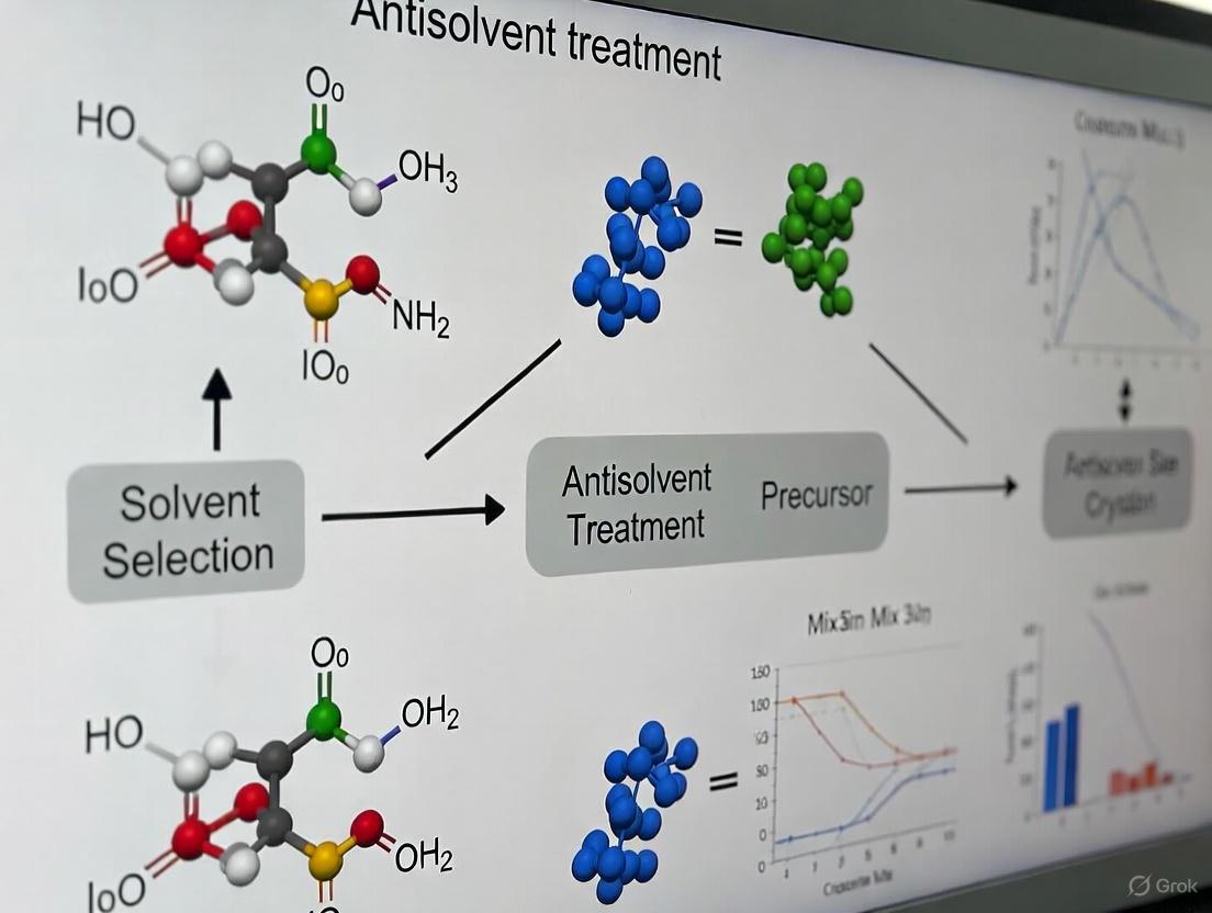
Antisolvent engineering is a cornerstone technique in the fabrication of high-performance perovskite solar cells (PSCs) and light-emitting diodes (PeLEDs). This process involves introducing a solvent, known as an antisolvent, into a perovskite precursor solution during spin-coating. The antisolvent, which is miscible with the precursor solvents but cannot dissolve the perovskite solutes, rapidly induces supersaturation by extracting the primary solvents. This triggers instantaneous nucleation and subsequent controlled crystal growth, leading to the formation of uniform and dense perovskite films. The meticulous selection of antisolvents based on key physicochemical properties—primarily polarity, miscibility, and boiling point—is paramount for controlling crystallization kinetics, final film morphology, and ultimately, the efficiency and stability of the resulting optoelectronic devices. This Application Note details these critical parameters and provides standardized protocols for their exploitation in perovskite research.
Core Physicochemical Properties
The effectiveness of an antisolvent is governed by a triad of interconnected physicochemical properties. Understanding their individual and collective roles is essential for rational antisolvent selection.
Polarity
Polarity is arguably the most critical parameter in antisolvent selection. It directly determines the antisolvent's capacity to precipitate the perovskite precursors from solution.
- Mechanism: The working principle of an antisolvent is its ability to reduce the overall solubility of the perovskite precursors (e.g., PbI₂, FAI, CsI) in the solvent mixture (typically DMF/DMSO). A lower polarity antisolvent decreases the solution's dielectric constant and solvation power, leading to rapid supersaturation and nucleation.
- Optimal Range: An ideal antisolvent should have a polarity in the approximate range of 2.0 to 4.5 [17]. Antisolvents with higher polarity increase perovskite solubility, resulting in insufficient precipitation, low film coverage, and uneven quality. Excessively low polarity can cause adverse effects, including unstable precursor solubility and overly rapid crystallization that is difficult to control [17].
Table 1: Polarity and Properties of Common Antisolvents
| Antisolvent | Boiling Point (°C) | GHS Hazard Category | Key Health Hazards | Primary Application |
|---|---|---|---|---|
| Diethyl carbonate | 126 | — | No known health hazards | Green antisolvent for PSCs [17] |
| Ethyl acetate (EA) | 77.2 | H336 | May cause drowsiness or vertigo | Common green antisolvent [17] |
| Anisole | 155 | H335 | May cause drowsiness or vertigo | Green, higher boiling point antisolvent [17] |
| Dimethyl sulfide (DMS) | ~37 (High vapor pressure) | — (Industry-compatible) | — | High-coordination solvent for bathing [18] |
| tert-Butanol (TBA) | ~82-83 | — | Low hazard | Cost-effective green antisolvent with wide processing window [19] |
| n-Hexane | ~69 | — | — | Slows crystallization for blue PeLEDs [20] |
| Chlorobenzene (CB) | 131 | H332 | Harmful if inhaled | Conventional toxic antisolvent (reference) [18] |
Miscibility
Miscibility refers to the ability of the antisolvent to mix homogeneously with the precursor solvents (DMF and DMSO). It governs the diffusion rate and uniformity of saturation across the film.
- Mechanism: High miscibility enables efficient and rapid extraction of DMF/DMSO from the wet perovskite film. This leads to a fast supersaturation spike, generating a high density of nucleation sites, which is beneficial for dense, pinhole-free films [18].
- Trade-offs: However, excessively high miscibility can lead to uncontrollably fast crystallization, introducing defects and causing film wrinkling. The miscibility is often temperature-dependent; for instance, lowering the temperature of diethyl ether (DE) reduces its miscibility with DMSO, allowing for precise control over wrinkle geometry in perovskite films [21].
- Application-Specific Tuning: The interaction between the perovskite precursor solution and the antisolvent can be regulated to achieve desired outcomes. For example, alkane antisolvents like n-hexane exhibit weak interactions with perovskite precursors, resulting in a slower crystallization rate. This is crucial for air-processed blue PeLEDs, as it enhances crystalline quality and reduces trap density [20].
Boiling Point
Boiling point influences the volatilization kinetics of the antisolvent during the subsequent annealing step, which affects the crystal growth and drying stress.
- Mechanism: After inducing nucleation, the residual antisolvent must be removed cleanly during thermal annealing. A moderate boiling point is often desirable. Very low-boiling-point antisolvents (e.g., diethyl ether, 34.6°C) may evaporate too quickly, complicating process control, while very high-boiling-point antisolvents may linger too long, interfering with crystal growth or creating voids.
- Green Antisolvent Consideration: Many green antisolvents, such as anisole (155°C) and ethyl lactate (154°C), possess higher boiling points than conventional toxic solvents like chlorobenzene (131°C) and toluene (111°C). This can provide a wider processing window but requires optimized annealing conditions [17].
The following diagram illustrates how these three core properties collectively influence the stages of perovskite film formation.
Experimental Protocols
Protocol: Standard Spin-Coating with Antisolvent Quenching
This protocol is for fabricating a standard pin-hole free FA-based perovskite film using a one-step spin-coating method with antisolvent quenching.
Research Reagent Solutions & Materials:
- Perovskite Precursor Solution: Formamidinium iodide (FAI), lead iodide (PbI₂), methylammonium chloride (MACl) in anhydrous DMF:DMSO (4:1 v/v).
- Antisolvent: Anhydrous ethyl acetate, chlorobenzene, or other selected antisolvent.
- Substrate: ITO/SnO₂ or ITO/PEDOT:PSS.
- Equipment: Spin coater, hot plate, programmable pipette, nitrogen gun (optional).
Procedure:
- Substrate Preparation: Clean the substrate with UV-ozone or oxygen plasma treatment for 15-20 minutes to ensure a hydrophilic surface.
- Spin-Coating:
- Dynamically dispense the perovskite precursor solution onto the spinning substrate.
- Spin-coat using a two-step program: 1000 rpm for 10 s (spread) followed by 4000-6000 rpm for 30 s (thin).
- Antisolvent Quenching:
- Precisely 5-10 seconds before the end of the high-speed spin step, rapidly drip 200-500 µL of antisolvent onto the center of the spinning substrate using a pipette [17]. The exact timing is composition-dependent and must be optimized.
- Thermal Annealing:
- Immediately transfer the film to a pre-heated hot plate. Anneal at 100°C for 10-30 minutes to facilitate perovskite crystallization and residual solvent evaporation.
- Cooling:
- After annealing, allow the sample to cool naturally to room temperature before further processing or characterization.
Protocol: Antisolvent Bathing (ASB) for Large Grains
The ASB technique is an industry-compatible, scalable method that promotes the growth of large-grained, high-quality perovskite films.
Research Reagent Solutions & Materials:
- Perovskite Precursor Solution: Cs₀.₂FA₀.₈Pb((I₀.₈₂Br₀.₁₈)₀.₉₇Cl₀.₀₃)₃ (3-hal) in DMF:DMSO.
- Coordination Antisolvent: Dimethyl sulfide (DMS) or Diethyl ether (DE) [18].
- Substrate: ITO/SnO₂.
- Equipment: Spin coater, hot plate, glass Petri dish.
Procedure:
- Film Deposition: Spin-coat the perovskite precursor solution onto the substrate using an optimized program without in-situ antisolvent dripping. The film will appear wet and translucent.
- Bathing:
- Immediately after spin-coating, carefully submerge the wet film into a Petri dish containing the antisolvent (e.g., DMS). Ensure the film is fully immersed.
- Leave the film to bathe for a defined period (e.g., 2 minutes). Observe the color change from translucent to dark brown, indicating intermediate phase formation and solvent extraction [18].
- Annealing:
- Remove the substrate from the bath and place it on a preheated hot plate. Anneal at an optimized temperature (e.g., 80°C) for a short period (e.g., 5 minutes) to complete the crystallization [18].
The Scientist's Toolkit
Table 2: Essential Research Reagents for Antisolvent Engineering
| Reagent / Material | Function / Purpose | Key Characteristics |
|---|---|---|
| Ethyl Acetate (EA) | A common green antisolvent for inducing nucleation. | Boiling point: 77.2°C; Moderate polarity; Hazard: H336 [17]. |
| Dimethyl Sulfide (DMS) | High-coordination solvent for ASB; promotes uniform nucleation. | High Gutmann donor number (40.0 kcal mol⁻¹); strong Pb²⁺ coordination [18]. |
| tert-Butanol (TBA) | Cost-effective green antisolvent with a wide processing window. | Hydrogen-bonds with DMF/DMSO; improves reproducibility [19]. |
| n-Hexane / n-Octane | Alkane antisolvent for slow crystallization (e.g., for blue PeLEDs). | Weak precursor interaction; reduces crystallization rate [20]. |
| Methylammonium Chloride (MACl) | Volatile additive in precursor solution. | Widens crystallization window; reduces α-phase formation energy [22]. |
| Trifluoroacetamide (TFAA) | Multifunctional volatile additive. | Coordinates with Pb²⁺; passivates defects; releases strain from MACl [22]. |
| Alumina (Al₂O₃) Particles | Nucleation site modifier on textured substrates. | Super-hydrophilic surface; lowers nucleation barrier for conformal coating [23]. |
The targeted selection and application of antisolvents based on their polarity, miscibility, and boiling point provide a powerful pathway to control perovskite crystallization. While conventional toxic antisolvents are still widely used in research, the development of effective green antisolvents like ethyl acetate, anisole, diethyl carbonate, and tert-butanol is critical for the future scalable and sustainable manufacturing of perovskite optoelectronics. The protocols outlined herein—from standard quenching to advanced bathing methods—offer a framework for reproducible fabrication of high-quality perovskite films. Future work will continue to refine our understanding of solvent-solute interactions and develop novel antisolvent systems that push the boundaries of device performance and stability.
A Practical Guide to Antisolvent Processing Parameters and Techniques
Antisolvent engineering is a critical processing technique for controlling the crystallization of advanced materials, finding essential applications in the fabrication of metal-halide perovskite semiconductors for photovoltaics and the production of nanodrugs in pharmaceutical development. The fundamental principle relies on inducing rapid supersaturation by introducing an "antisolvent"—a solvent in which the target material has limited solubility—into a precursor solution. This triggers uniform nucleation and controlled crystal growth, ultimately determining the morphological, structural, and optoelectronic properties of the final solid film or drug nanoparticle [24] [25]. In perovskite solar cells (PSCs), this method has enabled remarkable power conversion efficiencies exceeding 26%, while in pharmaceuticals, it facilitates the production of high-loading, excipient-free nanodrugs with enhanced bioavailability [15] [25].
The selection of an appropriate antisolvent is paramount, as its physicochemical properties—including miscibility with the host solvent, polarity, vapor pressure, and coordination strength—directly influence the crystallization kinetics, phase purity, defect density, and ultimately the performance and stability of the resulting product. This application note provides a structured framework for antisolvent selection, transitioning from traditional toxic solvents towards modern, sustainable alternatives, supported by quantitative data, detailed protocols, and practical guidelines for researchers and scientists.
Theoretical Framework and Selection Criteria
Fundamental Principles of Antisolvent Action
The antisolvent precipitation process is governed by three sequential steps: nucleation, particle growth, and agglomeration. The driving force is supersaturation (β), defined as the ratio of the compound concentration in the solvent-antisolvent mixture (C₀) to its equilibrium solubility (C): β = C₀ / C [25]. According to classical nucleation theory, a critical energy barrier (ΔG*) must be overcome for stable nuclei to form:
[ \Delta G^* = \frac{16\pi\gamma^3\Omega^2}{3k_B^2T^2(\ln\beta)^2} ]
where γ is the interfacial tension, Ω is the molecular volume, k_B is Boltzmann's constant, and T is temperature [25]. A higher β lowers ΔG*, promoting nucleation over growth and leading to smaller particles or crystal grains. The rate of nucleation (J) depends exponentially on β:
[ J = An \exp\left[-\frac{16\pi\gamma^3\Omega^2}{3kB^3T^3(\ln\beta)^2}\right] ]
The role of the antisolvent is to rapidly increase β by reducing C*, primarily through two mechanisms: 1) solvent displacement and 2) coordination with precursor ions [24] [18]. In solvent displacement, the antisolvent extracts the host solvent from the wet film, forcing solute precipitation. In coordination-based approaches, the antisolvent directly interacts with metal cations (e.g., Pb²⁺), forming intermediate adducts that modulate the crystallization pathway [18].
Hansen Solubility Parameters (HSP) as a Selection Tool
Hansen Solubility Parameters (HSP) provide a quantitative framework for predicting solvent-antisolvent miscibility and their interaction with solutes. HSP divide the cohesive energy density of a solvent into three components:
- δD (Dispersion forces): Related to non-polar, van der Waals interactions.
- δP (Polar interactions): Related to permanent dipole-permanent dipole interactions.
- δH (Hydrogen bonding): Related to hydrogen donor/acceptor capability.
Solvents with similar HSP are typically miscible. An effective antisolvent must be miscible with the host solvent but should significantly reduce the solubility of the target solute. The following table presents HSP values for common solvents and antisolvents, enabling rational selection based on their relative coordinates in the Hansen space [24].
Table 1: Hansen Solubility Parameters for Common Solvents and Antisolvents
| Solvent Name | Full Name | Type | δD [MPa¹/²] | δP [MPa¹/²] | δH [MPa¹/²] |
|---|---|---|---|---|---|
| DMF | Dimethylformamide | Solvent | 17.4 | 13.7 | 11.3 |
| DMSO | Dimethyl sulfoxide | Solvent | 18.4 | 16.4 | 10.2 |
| GBL | γ-butyrolactone | Solvent | 18.0 | 16.6 | 7.4 |
| Chlorobenzene | Chlorobenzene | Antisolvent | 19.0 | 4.3 | 2.0 |
| Toluene | Toluene | Antisolvent | 18.0 | 1.4 | 2.0 |
| Diethyl Ether | Diethyl ether | Antisolvent | 14.5 | 2.9 | 4.6 |
| Ethyl Acetate | Ethyl acetate | Antisolvent | 15.8 | 5.3 | 7.2 |
For effective crystallization control, the antisolvent should have a moderately different HSP profile from the host solvent to ensure controlled, rather than instantaneous, precipitation. A large difference in δP and δH often correlates with a strong solubility reduction for perovskite precursors or drug molecules [24].
Quantitative Comparison of Antisolvent Materials
The following tables summarize key properties, performance, and toxicity data for a range of traditional and emerging antisolvents, facilitating direct comparison for informed experimental design.
Table 2: Properties and Performance of Traditional and Green Antisolvents
| Antisolvent | BP (°C) | Dipole Moment (D) | Vapor Pressure | Common Applications | Reported Performance |
|---|---|---|---|---|---|
| Chlorobenzene (CB) | 131 | 1.7 | Low | Standard for PSCs [26] | High PCEs (>24%), common lab reference |
| Toluene | 111 | 0.4 | Medium | PSCs, triggers fast crystallization [26] | Good film uniformity, can be sensitive to timing |
| Diethyl Ether (DE) | 35 | 1.3 | Very High | PSCs, antisolvent bathing [18] | Used in bathing methods, requires careful handling |
| Ethyl Acetate (EA) | 77 | 1.9 | High | PSCs, greener alternative [26] | Superior ambient stability in films [26] |
| Dimethyl Sulfide (DMS) | 37-39 | ~1.5 | High | Coordination-solvent bathing for PSCs [18] | PCE 20.6%, large grains (444 nm), high coordination |
| Ethanol | 78 | 1.7 | Medium | AVC of CsPbBr₃ single crystals [27] | Enables cm-scale, phase-pure single crystals |
| 2-MeTHF | 80 | 1.4 | Medium | Green solvent for 2D precursor phases [28] | Enables stable α-FAPbI₃ under ambient processing |
Table 3: Toxicity and Sustainability Profile of Antisolvents
| Antisolvent | Toxicity Profile | Green Credentials / Alternatives | Recommended Safety Precautions |
|---|---|---|---|
| Chlorobenzene | Harmful, suspected reproductive toxicant [29] | Avoid for large-scale use | Use in fume hood, avoid skin contact |
| Toluene | Reproductive toxicity, flammable [29] | Avoid for large-scale use | Use in fume hood, proper respiratory protection |
| Diethyl Ether | Extremely flammable, forms explosive peroxides | High risk, not green | Use in spark-free environment, store safely, test for peroxides |
| Ethyl Acetate | Low toxicity, recognized as a greener option [26] | Recommended greener alternative | Good laboratory ventilation generally sufficient |
| 2-MeTHF | Low toxicity, biorenewable [28] | Recommended green solvent | Class 3 solvent (low toxic potential) [28] |
| DMS | Industry-compatible, low-toxicity profile [18] | Promising for scalable fabrication | Standard laboratory ventilation required |
Detailed Experimental Protocols
Protocol 1: Standard Antisolvent Dripping for Perovskite Films
This protocol is adapted from procedures used to fabricate high-efficiency (>26%), methylammonium-free perovskite solar cells using Br-TPP porphyrin additive in the antisolvent [15].
Research Reagent Solutions
- Perovskite Precursor Solution: CsI, FAI, PbI₂, and PbBr₂ dissolved in a mixture of DMF and DMSO (4:1 v/v).
- Antisolvent Solution: Chlorobenzene or Toluene with/without functional additives (e.g., 0.5 mg/mL meso-tetra(4-bromophenyl) porphine (Br-TPP)).
- Substrate: ITO/SnO₂ or other charge transport layer-coated glass.
Step-by-Step Procedure
- Solution Preparation: Prepare the perovskite precursor solution (e.g., CsₓFA₁₋ₓPbI₃) in a nitrogen-filled glovebox (O₂ & H₂O < 1 ppm). Stir for 2-4 hours at 50°C until fully dissolved. Filter through a 0.22 µm PTFE syringe filter [15] [26].
- Spin-Coating: Dispense the precursor solution onto the pre-heated (e.g., 100°C) substrate. Initiate a two-step spin-coating program (e.g., 1000 rpm for 10 s, followed by 4000 rpm for 20 s).
- Antisolvent Dripping: 5-10 seconds before the end of the second spin-coating step, pipette 100-200 µL of the antisolvent (e.g., chlorobenzene with Br-TPP) steadily onto the center of the spinning substrate [15] [26]. Ensure uniform coverage.
- Annealing: Transfer the film immediately to a hotplate and anneal at 100-150°C for 10-30 minutes to remove residual solvents and complete crystallization.
- Characterization: The resulting film should be uniform and pinhole-free. Characterize by SEM (for morphology), XRD (for crystallinity), and UV-Vis/PL (for optoelectronic properties).
Critical Parameters
- Timing: The antisolvent dripping timing is crucial and must be optimized for each setup (typically during the last 5-15 s of spinning) [24].
- Volume: Insufficient volume leads to incomplete crystallization; excess volume can wash away the precursor.
- Environment: Controlled ambient (e.g., low humidity) is often required for reproducible results with traditional solvents [26].
Protocol 2: Green Antisolvent Bathing for Scalable Processing
This protocol utilizes the antisolvent bathing (ASB) method with a high-coordination, industry-compatible solvent like Dimethyl Sulfide (DMS) for methylammonium-free triple halide perovskites [18].
Research Reagent Solutions
- Perovskite Precursor Solution: Cs₀.₂FA₀.₈Pb((I₀.₈₂Br₀.₁₈)₀.₉₇Cl₀.₀₃)₃ dissolved in DMF/DMSO.
- Bathing Antisolvent: Anhydrous Dimethyl Sulfide (DMS).
- Substrate: ITO/SnO₂.
Step-by-Step Procedure
- Film Deposition: Spin-coat the perovskite precursor solution onto the substrate using a standard recipe (e.g., 4000 rpm for 30 s).
- Antisolvent Bathing: Immediately after spin-coating, submerge the wet film entirely in a bath of DMS for 2 minutes. Observe the color change from green/transparent to dark brown, indicating crystallization and solvent exchange [18].
- Thermal Annealing: Remove the film from the bath and transfer it to a pre-heated hotplate. Anneal at an optimized temperature (e.g., 80°C) for a short duration (5 minutes).
- Characterization: The resulting films show large grains (444 ± 122 nm), preferred (001) orientation, and enhanced electron diffusion lengths (up to 3 µm) [18].
Advantages for Scalability
- The ASB method is more reproducible and compatible with roll-to-roll processing than dripping.
- DMS has a high vapor pressure and strong coordination ability, enabling efficient removal of the host solvent (DMSO) and rapid crystallization with short, low-temperature annealing [18].
Protocol 3: Antisolvent Vapor-Assisted Crystallization (AVC) for Single Crystals
This protocol guides the growth of centimeter-scale CsPbBr₃ single crystals, a technique also applicable to other metal halide perovskites and crystalline materials [27].
Research Reagent Solutions
- Precursor Solution: CsBr and PbBr₂ (with 1.5x excess PbBr₂ to suppress Cs₄PbBr₆ phase) dissolved in a 9:1 (v/v) DMSO/DMF binary solvent to form a 0.35 M stock solution.
- Antisolvent: Ethanol.
Step-by-Step Procedure
- Precursor Preparation: Stir the precursor mixture at 50°C for 2 hours until fully dissolved. Filter through a 0.22 µm PTFE syringe filter.
- Metastable State Induction (Optional but recommended): Pre-titrate the clear stock solution with ethanol until the onset of turbidity. Re-filter to obtain a clear, metastable precursor solution. This step enhances the control over nucleation [27].
- Growth Vessel Setup: Place an aliquot of the precursor solution (e.g., 5-10 mL) into a vial. Place this vial open inside a larger, sealed container containing 20-50 mL of ethanol (the antisolvent).
- Crystal Growth: Store the entire setup at room temperature, undisturbed, for 5-7 days. Ethanol vapor slowly diffuses into the precursor solution, uniformly increasing supersaturation and promoting the growth of large, high-quality single crystals.
- Crystal Harvesting: Carefully extract the crystals, wash with DMF to remove surface residue, and air-dry.
Critical Parameters
- Solvent Selection: The DMSO/DMF ratio and ethanol as antisolvent were chosen based on Gutmann's donor numbers and Hansen Solubility Parameters to balance solubility and crystallization kinetics [27].
- Diffusion Control: Using vapor diffusion instead of direct liquid addition allows for much slower and more controlled supersaturation, which is key to growing large single crystals instead of polycrystalline powders.
The Scientist's Toolkit: Essential Research Reagents
Table 4: Key Reagent Solutions for Antisolvent Engineering
| Reagent / Material | Typ Function in Antisolvent Processes | Example Application / Note |
|---|---|---|
| DMF (Dimethylformamide) | Primary solvent for perovskite precursors/drug molecules. | Highly toxic; target for replacement in green processes [29] [28]. |
| DMSO (Dimethyl sulfoxide) | Coordinating solvent, forms intermediate adducts with Pb²⁺. | Less toxic than DMF but a skin penetration enhancer [30] [28]. |
| Chlorobenzene | Traditional lab-scale antisolvent for fast crystallization. | Being phased out due to toxicity; suitable for initial R&D [29] [26]. |
| Ethyl Acetate | Lower-toxicity antisolvent alternative. | Shows excellent ambient stability for perovskite films [26]. |
| 2-MeTHF | Biorenewable, low-toxicity solvent/antisolvent. | Ideal for green manufacturing; Class 3 solvent [28]. |
| DMI (1,3-Dimethyl-2-imidazolidinone) | Low-toxicity main solvent for precursor solutions. | Can form stable adducts with PbI₂; green alternative to DMF [30]. |
| Br-TPP (Porphyrin Derivative) | Functional additive in antisolvent for crystallization control. | Passivates defects, improves charge transport in PSCs [15]. |
| Butylamine (BA) | Co-solvent and component for 2D precursor phases. | Enables 2D-to-3D perovskite conversion under ambient air [28]. |
Workflow and Decision Pathways
The following diagram illustrates the logical decision process for selecting an appropriate antisolvent strategy, integrating both performance and sustainability considerations.
Diagram 1: Antisolvent Selection Workflow
The strategic selection of antisolvents has evolved from a reliance on traditional, toxic solvents towards a rational design incorporating modern, green alternatives. This transition is critical for the sustainable commercialization of perovskite photovoltaics and the environmentally friendly production of pharmaceuticals. The theoretical framework provided by Hansen Solubility Parameters and crystallization kinetics offers a scientific basis for solvent selection, moving beyond empirical trial-and-error.
Future development will focus on deepening the understanding of solvent-antisolvent-cation molecular interactions to design even more effective green solvents. The integration of machine learning with high-throughput experimental screening shows great promise for rapidly optimizing antisolvent systems and process parameters, accelerating the discovery of novel, sustainable crystallization pathways [26]. By adopting the guidelines, protocols, and green alternatives outlined in this application note, researchers can contribute to advancing both the performance and sustainability of their materials and processes.
Antisolvent treatment is a critical step in the processing of high-quality perovskite thin films for optoelectronic devices. This technique enables precise control over the crystallization kinetics by rapidly triggering nucleation and influencing crystal growth. The core principle involves the introduction of a solvent, in which the perovskite precursors are insoluble, into a deposited precursor solution. This rapidly induces supersaturation, a fundamental driver of crystallization [31]. The quality of the resulting film—including its coverage, crystallinity, and defect density—is exquisitely sensitive to the processing parameters of the antisolvent, namely its application timing, drip rate, applied volume, and temperature [32]. Mastering these parameters is therefore essential for fabricating efficient and stable perovskite solar cells and light-emitting diodes (PeLEDs). Inconsistent or suboptimal application can lead to defects such as pinholes, excessive roughness, or uncoordinated Pb²⁺ ions, which act as non-radiative recombination centers and significantly impede device performance [32].
Quantitative Parameter Relationships and Data Tables
The following tables summarize the key quantitative relationships and experimental parameters critical for antisolvent process optimization.
Table 1: Fundamental Crystallization Equations Governing Antisolvent Treatment
| Parameter | Mathematical Expression | Description & Role in Antisolvent Treatment |
|---|---|---|
| Supersaturation (ΔC) | ΔC = C - C₀ [31] |
Represents the driving force for nucleation. Antisolvent application rapidly decreases equilibrium concentration (C₀), causing a spike in ΔC. Precise control over this spike is key. |
| Critical Nucleus Radius (r_c) | r_c = 2γ / ΔG_v [31] |
The minimum stable nucleus size. Higher supersaturation lowers r_c, promoting a high nucleation density for dense, pinhole-free films. |
| Nucleation Rate (J) | J = A exp(-ΔG / (k_B T)) [31] |
The rate at which stable nuclei form. It is exponentially dependent on the energy barrier (ΔG). Antisolvent parameters directly modulate ΔG and thus J. |
Table 2: Optimization of Key Antisolvent Processing Parameters
| Parameter | Typical Range / Values | Impact on Film Morphology & Device Performance | Optimization Guideline |
|---|---|---|---|
| Application Timing | 5 - 15 seconds after spin-coating start [32] | Too early: Leads to incomplete solvent evaporation, small grains. Too late: Precursor solution dries, leading to rough, polycrystalline films with poor coverage. | Correlate with solution transparency and solvent evaporation rate. The optimal window is when the solution is saturated and ready for nucleation trigger. |
| Drip Rate | 0.5 - 2 mL/s (varies with volume) | Too fast: Creates excessive localized supersaturation, leading to many small nuclei and a high density of small grains. Too slow: Results in non-uniform crystallization across the substrate. | A steady, controlled rate ensures uniform nucleation conditions across the entire substrate. Automated syringe pumps are recommended for reproducibility. |
| Applied Volume | 0.5 - 2 mL for a 2x2 cm substrate | Insufficient: Fails to fully initiate crystallization, leaving residual solvents. Excessive: Can wash away precursors or cause delamination, creating pinholes and defects. | The volume must be sufficient to fully contact and treat the entire precursor film without pooling. |
| Antisolvent Temperature | 20 - 70 °C (for common antisolvents) | Lower T: Slows crystal growth kinetics, can lead to denser films. Higher T: Can accelerate growth and reduce defect density but may also promote non-uniform grain size. | Can be used in tandem with heated substrates to fine-tune growth dynamics after the initial nucleation burst. |
Experimental Protocol: Standardized Antisolvent Treatment for Perovskite Films
This protocol details a generalized procedure for the antisolvent-assisted deposition of a perovskite thin film (e.g., MAPbI₃ or FAPbI₃), adaptable for solar cell or LED fabrication.
Materials and Reagent Solutions
Table 3: Essential Research Reagents and Materials
| Item | Function / Role in the Process |
|---|---|
| Perovskite Precursor Solution (e.g., 1.2M MAI:PbI₂ in DMF:DMSO) | The source of cations (MA⁺, FA⁺, Cs⁺) and anions (Pb²⁺, I⁻, Br⁻) for crystal formation. DMSO coordinates with PbI₂, slowing crystallization. |
| Antisolvents (e.g., Chloroform, Toluene, Diethyl Ether) | A solvent miscible with the host solvent (DMF/DMSO) but non-solvent for perovskite. Rapidly extracts host solvent, inducing supersaturation and nucleation. |
| Polymeric Additives (e.g., PEO, PEG) [32] | Increase precursor solution viscosity, restricting precursor diffusion and leading to smaller, more uniform crystal grains. Passivate surface defects. |
| Defect Passivation Agents (e.g., TMPTA) [32] | Molecules with functional groups (e.g., C=O) that bind to uncoordinated Pb²⁺ ions, suppressing non-radiative recombination and improving luminescence. |
| Substrate (ITO/Glass with HTL, e.g., PEDOT:PSS) [32] | Provides a conductive, smooth surface for film deposition and charge injection/collection. |
Step-by-Step Procedure
- Substrate Preparation: Clean the patterned ITO/glass substrates sequentially in Hellmanex solution, deionized water, acetone, and isopropanol via ultrasonication for 15 minutes each. Treat with UV-Ozone for 20 minutes to improve wettability.
- Hole Transport Layer (HTL) Deposition: Spin-coat the PEDOT:PSS solution at 4000 rpm for 30 seconds, then anneal at 150 °C for 15 minutes in air. Transfer to a nitrogen-filled glovebox for subsequent steps.
- Perovskite Precursor Preparation: Dissolve stoichiometric quantities of formamidinium iodide (FAI), lead iodide (PbI₂), and methylammonium bromide (MABr) in a mixed solvent of anhydrous DMF and DMSO (4:1 v/v) to achieve a 1.3M concentration. Optional: Add controlled amounts of PEO (e.g., 0.1 mg/mL) and TMPTA (e.g., 0.5 vol%) for grain manipulation and defect passivation [32]. Stir at 60 °C for 2 hours until fully dissolved.
- Spin-Coating & Antisolvent Dripping:
- Dynamic Dispense: Pipette 80 µL of the perovskite precursor solution onto the center of the stationary substrate.
- Spin Program: Immediately initiate a two-step spin-coating program:
- Step 1: 1000 rpm for 10 seconds (spread acceleration).
- Step 2: 4000 rpm for 25 seconds (thin film acceleration).
- Critical Antisolvent Application: Using a precision syringe, rapidly drip 1.0 mL of toluene at a rate of 1 mL/s onto the center of the spinning substrate at 5 seconds before the end of the spin program (i.e., at the 20-second mark of a 25-second second step).
- Thermal Annealing: Immediately after spin-coating, transfer the wet film to a hotplate and anneal at 100 °C for 45 minutes to facilitate crystal growth and solvent removal, forming a dense, dark brown perovskite film.
- Post-Fabrication & Characterization: Complete device fabrication by thermally evaporating electron transport and electrode layers. Characterize film quality using scanning electron microscopy (SEM) for morphology, photoluminescence (PL) spectroscopy for optoelectronic properties, and X-ray diffraction (XRD) for crystallinity.
Advanced Optimization and Data-Driven Parameter Control
Beyond empirical tuning, systematic and data-driven approaches are crucial for robust parameter optimization.
Response Surface Methodology (RSM)
RSM is a powerful statistical technique for modeling and optimizing multiple parameters simultaneously. It can be used to build a predictive model that relates antisolvent parameters (e.g., timing, volume) to a performance output (e.g., Power Conversion Efficiency, PCE) [33]. The resulting regression equations and contour plots can precisely identify the optimal parameter set and reveal interaction effects that are not apparent in one-factor-at-a-time experiments.
Inline Process Analytical Technology (PAT)
Integrating real-time monitoring tools like Near-Infrared (NIR) spectroscopy with process parameters (spinner speed, temperature) enables superior prediction and control of Critical Quality Attributes (CQAs) like final particle size and moisture content [34]. A merged Partial Least Squares (PLS) model that uses both NIR spectra and process parameters has been shown to outperform models using either data source alone, providing a more accurate endpoint prediction for granulation processes, a concept directly transferable to perovskite film formation [34].
Process Visualization and Workflow
The following diagram illustrates the logical sequence and decision points involved in the antisolvent crystallization process.
Antisolvent Crystallization Workflow
The nucleation and crystal growth dynamics governed by the processing parameters can be summarized by the following conceptual diagram.
Crystallization Dynamics and Parameter Influence
Antisolvent engineering is a cornerstone technique in the fabrication of advanced materials, particularly in the fields of perovskite photovoltaics and pharmaceutical crystallization. The process, which involves introducing a solvent that reduces the solubility of a solute to induce crystallization, is critical for controlling film morphology and crystal quality. Recent research has demonstrated that the rate of antisolvent application is a pivotal, yet often overlooked, parameter that profoundly influences the final material's properties [6]. This application note delineates a formal categorization of antisolvents into three distinct types—Type I (Fast), Type II (Neutral), and Type III (Slow)—based on their performance response to application rate. This framework provides researchers and process engineers with a systematic methodology to select and optimize antisolvents for specific applications, thereby enhancing the reproducibility and performance of crystalline materials.
Classification and Impact of Antisolvent Types
The categorization of antisolvents is predicated on the relationship between their application rate during spin-coating and the resulting performance of the fabricated devices or crystals. This classification is universal across a wide range of antisolvent chemistries [6].
Quantitative Classification Criteria
Table 1: Categorization of Common Antisolvents and Their Performance Characteristics [6]
| Antisolvent Type | Representative Antisolvents | Optimal Application Rate | Impact of Incorrect Application Rate | Key Performance Metrics (Optimal Conditions) |
|---|---|---|---|---|
| Type I (Fast) | Ethanol, Isopropyl Alcohol (IPA), Butanol | Fast (~1100-1500 µL/s) | Severe performance degradation; reduced PCE, broader parameter distribution [6]. | PCE: >21%, VOC: ~1.1 V, FF: 75-83% [6]. |
| Type II (Neutral) | Chlorobenzene, Toluene, Acetonitrile | Broad Range (100-1500 µL/s) | Minimal performance impact; robust to application variance [6]. | PCE: ~21%, VOC: ~1.1 V, FF: 75-83% [6]. |
| Type III (Slow) | Mesitylene, Ethyl Acetate, Diethyl Ether | Slow (~100-150 µL/s) | Non-functional devices or significantly worsened performance [6]. | PCE: >21%, VOC: ~1.1 V, FF: 75-83% [6]. |
Underlying Physicochemical Principles
The type-specific behavior is governed by two fundamental antisolvent properties:
- Solubility of Organic Precursors: The antisolvent's capacity to dissolve the organic components (e.g., methylammonium iodide, formamidinium iodide) of the perovskite precursor solution [6].
- Miscibility with Host Solvent: The degree of miscibility between the antisolvent and the primary solvent(s) (e.g., DMF, DMSO) of the perovskite precursor ink [6].
These properties combine to dictate the rate-dependent kinetics of solvent displacement, intermediate phase formation, and ultimate crystallization during the antisolvent application step.
Figure 1: A decision pathway for classifying antisolvents and determining the optimal application rate based on key physicochemical properties.
Experimental Protocols for Antisolvent Categorization
This section provides a detailed, step-by-step methodology for classifying an unknown antisolvent and fabricating optimized perovskite films based on its type.
Protocol A: Determining Antisolvent Application Rate
Objective: To empirically determine the optimal application rate (fast, slow, or neutral) for a novel antisolvent.
Materials:
- Perovskite precursor solution (e.g., triple-cation Cs₀.₀₅(MA₀.₁₇FA₀.₈₃)₀.₉₅Pb(I₀.₉Br₀.₁)₃ in DMF/DMSO)
- Antisolvent under test
- Substrates (e.g., ITO/glass with electron transport layer)
- Spin coater
- Two micropipettes (e.g., 250 µL and 1000 µL sizes)
- High-speed camera (optional, for rate verification)
Procedure:
- Solution Preparation: Prepare the perovskite precursor solution according to established stoichiometric methods and filter (0.22 µm PTFE filter) before use [6].
- Fast Application: a. Dispense the precursor solution onto the substrate and initiate spin-coating (e.g., 5000 rpm). b. At a predetermined delay (e.g., 5-10 seconds before the end of the spin cycle), rapidly dispense 200 µL of antisolvent using the 1000 µL pipette. The target extrusion rate is ~1100 µL/s [6]. c. Complete the spin cycle and proceed to thermal annealing.
- Slow Application: a. On a fresh substrate, repeat the spin-coating process. b. At the same delay, slowly dispense 200 µL of the same antisolvent using the 250 µL pipette. The target extrusion rate is ~150 µL/s [6]. c. Complete the spin cycle and proceed to thermal annealing.
- Analysis and Categorization: a. Characterize the resulting films via scanning electron microscopy (SEM) for morphology and X-ray diffraction (XRD) for crystallinity. b. Fabricate full devices and measure photovoltaic performance (J-V curves). c. Categorize the antisolvent: - Type I (Fast): Devices from Step 2 perform significantly better. - Type II (Neutral): Devices from Steps 2 and 3 show comparable performance. - Type III (Slow): Devices from Step 3 perform significantly better.
Protocol B: Optimized Film Fabrication via SACR Strategy
Objective: To fabricate high-quality, single-orientation perovskite films using the Solvent-Additive Cascade Regulation (SACR) strategy, incorporating antisolvent engineering [35].
Materials:
- Lead iodide (PbI₂)
- Formamidinium iodide (FAI), Cesium Iodide (CsI)
- Solvents: DMF, DMSO, NMP
- Additives: Cyclohexylamine (CHA), Cyclohexylamine Iodide (CHAI)
- Antisolvent (e.g., Chlorobenzene, Type II)
Procedure:
- Precursor and Additive Solution Preparation: a. Prepare a 1.5M PbI₂ solution in two different solvent systems: System A: DMF/DMSO (4:1 v/v) and System B: DMF/NMP (4:1 v/v) [35]. b. Prepare an organic cation solution: FAI/CsI in isopropanol. c. Prepare additive solutions: 5 mM CHA in IPA for System A, and 5 mM CHAI in IPA for System B [35].
- Two-Step Deposition with SACR: a. Step 1 - PbI₂ Coating: Spin-coat the PbI₂ solution (from System A or B) onto the substrate. During spinning, apply the chosen antisolvent at its optimal rate (from Protocol A). b. Step 2 - Conversion: Immediately spin-coat the FAI/CsI solution onto the PbI₂ film. c. Additive Treatment: Before annealing, spin-coat the corresponding additive solution (CHA for System A, CHAI for System B) to direct final crystal facet orientation [35]. d. Thermal Annealing: Anneal the film at 100°C for 30 minutes to form the final perovskite layer.
- Outcome: Using System A with CHA yields homogeneous (111)-oriented films. Using System B with CHAI yields homogeneous (100)-oriented films, both with high performance and stability [35].
Figure 2: Experimental workflow for the Solvent-Additive Cascade Regulation (SACR) strategy, integrating antisolvent application with facet-direction additives for single-oriented perovskite films [35].
The Scientist's Toolkit: Essential Research Reagents and Materials
Table 2: Key Reagents and Materials for Antisolvent Crystallization Research
| Item Name | Function/Application | Representative Examples |
|---|---|---|
| Polar Aprotic Solvents | Host solvents for perovskite precursors; coordination with Pb²⁺ dictates intermediate phases [36] [35]. | Dimethylformamide (DMF), Dimethyl Sulfoxide (DMSO), N-Methyl-2-pyrrolidone (NMP) [35] [27]. |
| Type I (Fast) Antisolvents | Induce crystallization with fast application; often alcohols with high organic precursor solubility [6]. | Ethanol, Isopropyl Alcohol (IPA), Butanol [6]. |
| Type II (Neutral) Antisolvents | Robust, versatile antisolvents with wide application rate tolerance; most commonly reported [6]. | Chlorobenzene, Toluene [6]. |
| Type III (Slow) Antisolvents | Require slow application for optimal film formation; often esters or ethers [6]. | Mesitylene, Ethyl Acetate, Diethyl Ether [6]. |
| Facet-Directing Additives | Regulate specific crystal facet growth through differential bonding with crystal nuclei [35]. | Cyclohexylamine (CHA), Cyclohexylamine Iodide (CHAI) [35]. |
| Defect-Passivating Additives | Suppress ion mobility and passivate defects at grain boundaries, reducing J-V hysteresis [36]. | Potassium Halide Salts (e.g., KI, KCl) [36]. |
The pursuit of high-performance perovskite solar cells (PSCs) has intensified the focus on controlling perovskite crystallization kinetics and thermodynamics. The quality of the perovskite thin film—including its crystallinity, grain size, morphology, and defect density—directly governs the optoelectronic properties and environmental stability of the resulting devices [26] [37]. This document details three advanced crystallization techniques—anti-solvent bathing, vapor-assisted crystallization, and additive engineering—that enable precise manipulation of the perovskite formation process. These methods facilitate the fabrication of large-grained, densely packed, and low-defect perovskite films, pushing power conversion efficiencies (PCEs) beyond 24% in laboratory-scale devices and offering pathways toward commercially viable production [38] [39].
The fundamental challenge in perovskite crystallization lies in managing the rapid reaction between organic cations and metal halides, which often leads to disordered nucleation, incomplete surface coverage, and high trap-state densities [37]. The techniques discussed herein address this by decoupling nucleation and growth stages, modulating crystallization kinetics, and passivating intrinsic defects, thereby bridging the gap between laboratory innovation and industrial manufacturing.
Comparative Analysis of Advanced Crystallization Techniques
Table 1: Performance characteristics of advanced crystallization techniques.
| Technique | Key Mechanism | Reported PCE (%) | Grain Size Enhancement | Primary Defect Mitigation | Scalability Potential |
|---|---|---|---|---|---|
| Anti-Solvent Bathing | Solvent extraction & supersaturation control | 24.49 [38] | Large grains (444 ± 122 nm) [40] | Reduces pinholes & grain boundaries [41] | High (compatible with R2R) [38] |
| Vapor-Assisted Crystallization | Conversion via vapor-phase reaction | N/A in provided results | Enables single-crystal thin films [42] | Eliminates grain boundaries [42] | Medium (requires controlled atmosphere) |
| Additive Engineering | Coordination with precursors & defect passivation | 23.02 [43] | Enlarged grains, less boundaries [44] | Passivates ionic defects [44] [1] | High (easily integrated into existing processes) |
Table 2: Key research reagents and materials for perovskite crystallization studies.
| Reagent/Material | Function/Application | Specific Examples |
|---|---|---|
| Anti-Solvents | Induce supersaturation by reducing precursor solubility | Chloroform [38], Toluene, Ethyl Acetate, Diethyl Ether, Chlorobenzene [26] |
| Lewis Base Additives | Coordinate with Pb²⁺ to form intermediate adducts, modulating crystallization | Dimethyl Sulfoxide (DMSO) [43] [41], 1-3-methylImidazole iodized salt (DMII) [44] |
| Reactive Additives | Undergo in-situ chemical reactions to release crystallization modifiers | trans-cinnamoyl chloride (TCC) [43] |
| Ionic Liquid Additives | Facilitate coarsening grain growth, enhance ion mobility, and passivate defects | DMII [44], Trimethylammonium Chloride [44] |
Anti-Solvent Bathing
Principle and Mechanism
Anti-solvent bathing is a crystallization technique wherein a substrate coated with a perovskite precursor solution is immersed in a poor solvent (anti-solvent) for the perovskite material. The primary mechanism involves the swift interdiffusion of the precursor solvent and the anti-solvent, which rapidly reduces the solubility of the perovskite precursors, triggering a high degree of supersaturation and initiating homogeneous nucleation [38] [41]. This method is particularly noted for its ultra-wide processing window (e.g., 10 seconds to 10 minutes bathing duration) and exceptional tolerance to post-bathing delay, making it highly robust and suitable for industrial-scale roll-to-roll (R2R) manufacturing where static wet films are prevalent [38]. Unlike spin-coating with anti-solvent dripping, the bathing approach provides a more uniform and controllable environment for the static wet film, leading to superior reproducibility.
Experimental Protocol
Protocol: Anti-Solvent Bathing for Static Perovskite Wet Films
Materials:
- Precursor solution: e.g., 1M MAPbI₃ in DMF:DMSO (4:1 v/v)
- Anti-solvent: e.g., Chloroform (CF) or Alkyl chlorides [38]
- Substrates: FTO or ITO-coated glass, pre-cleaned
- Nitrogen gas for drying
Procedure:
- Film Deposition: Deposit the perovskite precursor solution onto the substrate using a scalable method such as drop-coating, blade-coating, or slot-die coating to form a static wet film. Spin-coating can be used for lab-scale validation.
- Anti-Solvent Immersion: Immediately after deposition, immerse the substrate with the wet film into the anti-solvent bath (e.g., Chloroform). Maintain immersion for a controlled duration (e.g., 10 s to 10 min) [38].
- Solvent Removal: Remove the substrate from the bath. The anti-solvent and precursor solvents will interdiffuse, leading to immediate film darkening, indicating perovskite nucleation and crystallization initiation.
- Annealing: Transfer the substrate to a hotplate and anneal at 100°C for 10-15 minutes to remove residual solvents and complete the crystallization process, forming a compact, polycrystalline perovskite film.
Key Parameters & Optimization:
- Anti-Solvent Selection: Optimal anti-solvents like chloroform facilitate efficient solvent extraction and yield high-quality films with high PCE (e.g., 24.49%) [38]. Other options include ethyl acetate, which has demonstrated superior stability in ambiently fabricated films [26].
- Bathing Duration: The wide processing window (10 s to 10 min) enhances process robustness and reproducibility [38].
- Ambient Conditions: This method demonstrates exceptional resilience to humidity (30-50% RH), allowing for fabrication in ambient air [38].
Figure 1: Anti-solvent bathing experimental workflow for static wet films.
Vapor-Assisted Crystallization
Principle and Mechanism
Vapor-assisted crystallization is a two-step process that separates the deposition of the inorganic framework (e.g., PbI₂) from its conversion to the perovskite phase. The method involves exposing a pre-deposited inorganic film to a vapor containing the organic cations (e.g., methylammonium iodide, MAI). The organic vapor diffuses into the solid inorganic film, initiating a solid-state reaction that converts it into perovskite [42]. This technique leverages slow, controlled diffusion from the vapor phase to facilitate the growth of high-quality perovskite layers with superior crystallinity, reduced defect density, and the potential for forming large-area single-crystal thin films (SCTFs) by minimizing nucleation sites and promoting oriented crystal growth [42]. The absence of solvent during the conversion phase eliminates solvent-related issues such as porosity and poor morphology control.
Experimental Protocol
Protocol: Vapor-Assisted Crystallization for Perovskite Films
Materials:
- Inorganic precursor: PbI₂ solution (e.g., in DMF)
- Organic precursor: e.g., MAI or FAI powder
- Sealed container or reactor
- Hotplates
Procedure:
- Inorganic Layer Deposition: Deposit a thin, compact film of PbI₂ onto the substrate via spin-coating or other deposition techniques. Anneal the film to form a solid layer.
- Vapor Exposure Setup: Place the PbI₂-coated substrate and a separate crucible containing the organic halide powder (e.g., MAI) inside a sealed container.
- Heating and Conversion: Place the entire sealed container on a hotplate. Heat the system to a temperature that generates sufficient organic halide vapor pressure (e.g., 150-200°C). The vaporized organic molecules diffuse to and react with the PbI₂ film, converting it to perovskite (e.g., MAPbI₃). The conversion time can range from minutes to hours, depending on the temperature and film thickness.
- Cooling and Completion: After the reaction is complete (typically indicated by a color change to dark brown/black), turn off the heat and allow the system to cool naturally to room temperature before removing the substrate.
Key Parameters & Optimization:
- Vapor Pressure Control: The organic precursor temperature determines vapor pressure, affecting reaction kinetics and film quality [42].
- Inorganic Film Morphology: The porosity and crystallinity of the initial PbI₂ film are critical, as they govern the diffusion of organic vapor and the completeness of the conversion reaction [42].
- Reaction Temperature and Time: Higher temperatures accelerate the reaction but may introduce defects or degrade the organic cation. Optimization is required to balance conversion speed and film quality [42].
Figure 2: Vapor-assisted crystallization workflow for perovskite film formation.
Additive Engineering
Principle and Mechanism
Additive engineering involves incorporating small quantities of molecular or ionic compounds into the perovskite precursor solution to influence crystallization kinetics, modulate grain growth, and passivate electronic defects. The mechanisms of action are diverse: Lewis base additives (e.g., DMSO) coordinate with Pb²⁺ ions to form stable intermediate complexes, retarding crystallization and facilitating the growth of larger grains [1] [41]. Ionic liquid additives (e.g., DMII) enhance ion mobility across grain boundaries, facilitating coarsening grain growth during annealing rather than affecting the initial nucleation phase [44] [1]. Furthermore, some additives function as passivating agents, interacting with undercoordinated ions at grain boundaries and surfaces to reduce trap-state densities and suppress non-radiative recombination [44] [43].
Experimental Protocol
Protocol: Incorporating DMII Additive via Anti-Solvent-Assisted Process
Materials:
- Precursor solution: MAI and PbI₂ in NMP and GBL
- Additive: 1-3-methylImidazole iodized salt (DMII)
- Anti-solvent: Diethyl ether
Procedure:
- Precursor Solution Preparation: Prepare the perovskite precursor solution by dissolving stoichiometric amounts of MAI and PbI₂ in a mixed solvent of N-methyl-2-pyrrolidinone (NMP) and γ-butyrolactone (GBL). Add a specific molar ratio (e.g., 1%) of DMII additive to the precursor solution and stir thoroughly until a clear solution is obtained [44].
- Spin-Coating: Deposit the precursor solution onto the substrate via a two-step spin-coating program (e.g., 1000 rpm for 10 s followed by 3000 rpm for 20 s).
- Anti-Solvent Dripping: During the second spin-coating step, at a precise moment (e.g., 5-10 s before the end), drip the anti-solvent (e.g., diethyl ether) onto the center of the spinning substrate to initiate rapid solvent extraction and nucleation [44].
- Annealing: Transfer the substrate immediately to a hotplate and anneal at 90-110°C for 10-15 minutes. During this stage, the additive mediates grain coarsening by enhancing ion mobility, leading to enlarged grain size and improved crystallinity [44] [1].
Key Parameters & Optimization:
- Additive Concentration: Optimal concentration is critical. For DMII, a 1% molar ratio significantly improved PCE from 12.80% to 14.56% [44]. Excess additive can deteriorate film quality.
- Coordination Strength: The donor number of the additive influences the strength of the lead complex, impacting the crystallization delay and final grain size [1].
- Additive Reactivity: Reactive additives like trans-cinnamoyl chloride (TCC) can undergo in-situ reactions (e.g., Kornblum reaction with DMSO) to generate new species that coordinate with Pb²⁺, offering an alternative pathway for crystallization control [43].
Figure 3: Additive engineering workflow for enhanced perovskite crystallization.
The advanced crystallization techniques detailed herein—anti-solvent bathing, vapor-assisted crystallization, and additive engineering—provide a robust toolkit for fabricating high-quality perovskite thin films with controlled microstructure and enhanced optoelectronic properties. Anti-solvent bathing stands out for its exceptional processing window and compatibility with scalable fabrication under ambient conditions. Vapor-assisted crystallization offers a unique pathway for growing high-purity, oriented films, including single-crystal thin films. Additive engineering delivers unparalleled control over crystallization kinetics and defect passivation, significantly boosting device performance and operational stability. The integration of these strategies, guided by a fundamental understanding of nucleation and crystal growth principles, is pivotal for advancing perovskite optoelectronics from laboratory research toward widespread commercial application.
Overcoming Synthesis Challenges: Defects, Orientation, and Reproducibility
Controlling Crystallization Kinetics to Minimize Pinholes and Reduce Defect Density
Controlling the crystallization kinetics of perovskite films is a fundamental aspect of producing high-performance and stable optoelectronic devices. Within the broader context of antisolvent treatment research, the precise manipulation of nucleation and growth phases is critical to obtaining uniform, pinhole-free films with low defect densities. Uncontrolled crystallization often leads to excessive pinholes and defects, which act as centers for non-radiative recombination and ion migration, ultimately degrading device performance and stability [45] [24]. This application note details the underlying principles and provides detailed protocols for controlling crystallization kinetics, focusing on antisolvent and antisolvent-free methods to achieve superior perovskite film quality.
Theoretical Foundations of Crystallization Kinetics
The formation of perovskite films involves two primary stages: nucleation and crystal growth. Achieving compact, uniform films requires a high nucleation density, whereas high crystal quality necessitates slow, controlled growth [45].
Nucleation and Growth Dynamics
In large-area coating methods like blade-coating, nucleation is typically heterogeneous. The energy barrier for heterogeneous nucleation (ΔGhetero*) and the nucleation rate are described by [45]:
$$ \varDelta {{G}_{{\rm{hetero}}}}^{\ast }=\frac{16{\rm{\pi}}}{3}\frac{{\sigma}^{3}{v}^{2}}{\varDelta {\mu}^{2}}\frac{2-3\,\cos \theta +{\cos}^{3}\theta}{4} $$
$$ \frac{{\rm{d}}{N}{{\rm{hetero}}}^{\ast }}{{\rm{d}}t}=\varGamma \exp\left[\frac{-16{\rm{\pi}} {\sigma}^{3}{v}^{2}}{3{k}{{\rm{B}}}T\varDelta {\mu}^{2}}\frac{2-3\,\cos \theta +{\cos}^{3}\theta}{4}\right] $$
Where σ is the interface energy, v is the critical nucleus volume, θ is the contact angle between the solution and substrate, Δμ is the chemical potential difference, kB is the Boltzmann constant, and T is temperature. These equations indicate that nucleation rate and density can be increased by elevating temperature, precursor concentration, or interface energy [45].
The crystal growth rate (R) is related to the rate of change of the solution's supersaturation concentration (ΔC) [45]:
$$ R=-\frac{{\rm{d}}\varDelta C}{{\rm{d}}t} $$
Slowing the solute precipitation rate delays crystal growth, allowing for the formation of larger, higher-quality grains. Therefore, the ideal crystallization pathway involves fast nucleation to ensure uniformity and compactness, followed by slow growth to maximize crystal quality [45].
The Role of Antisolvent in Crystallization
The solvent-engineering method uses an antisolvent to rapidly induce supersaturation. The antisolvent, typically a solvent in which perovskite precursors have low solubility, is applied during spin-coating to extract the host solvent (e.g., DMF, DMSO). This rapidly increases precursor concentration, triggering uniform nucleation [24]. The properties of the antisolvent—such as its miscibility with the host solvent, boiling point, and dipole moment—critically influence the dynamics of solvent extraction and the subsequent nucleation and growth processes [24].
Experimental Protocols
Protocol 1: Static Antisolvent Treatment for Two-Step Deposited MAPI Films
This protocol tailors the PbI₂ layer morphology using a static antisolvent approach to enhance the final perovskite film quality [46].
- Key Principle: Controlling the crystallinity of the PbI₂ layer through static antisolvent loading time governs the grain size and defect density in the resulting Methylammonium Lead Iodide (MAPI) film [46].
Materials:
- Precursors: Lead Iodide (PbI₂, 99.999%), Methylammonium Iodide (MAI, 99.99%)
- Solvents: Dimethylformamide (DMF), Dimethyl Sulfoxide (DMSO)
- Antisolvent: Chlorobenzene
- Substrate: Fluorine-doped Tin Oxide (FTO) coated glass
Procedure:
- PbI₂ Solution Preparation: Dissolve 461 mg of PbI₂ in 0.5 mL DMF and 0.2 mL DMSO.
- PbI₂ Deposition: Spin-coat the PbI₂ solution onto the FTO substrate (1000 RPM for 10 s, then 3000 RPM for 20 s).
- Static Antisolvent Application: At the 5-second mark of the second spinning step, pipette 100 µL of chlorobenzene onto the stationary substrate. Allow the antisolvent to reside on the film for a defined loading time (e.g., ~5 seconds).
- Conversion to Perovskite: Deposit the MAI solution to convert the PbI₂ layer to MAPI.
- Annealing: Transfer the substrate to a hotplate and anneal at 100°C for 10 minutes in ambient air.
Critical Parameters:
- Antisolvent Loading Time: An optimum of ~5 seconds yields the largest grain size and highest photoluminescence lifetime. Longer times decrease PbI₂ crystallinity and increase defect density in the final MAPI film [46].
Protocol 2: Gas Quenching for Wide-Bandgap Perovskite Films
This protocol utilizes a directed gas stream to initiate crystallization, serving as an alternative to antisolvent quenching for reduced wrinkling and pinhole formation [47].
- Key Principle: Gas quenching controls solvent removal and crystallization initiation mechanically, leading to lower wrinkle density and a more uniform surface topography compared to antisolvent quenching [47].
Materials:
- Perovskite Precursor: Cs₀.₁₅FA₀.₈₅Pb(I₀.₆Br₀.₄)₃ in a host solvent (e.g., DMF:DMSO mixture)
- Gas: Nitrogen (N₂), high purity
- Substrate: Planar electron transport layer (e.g., SnO₂)
Procedure:
- Perovskite Deposition: Spin-coat the perovskite precursor solution onto the substrate.
- Gas Quenching: During the final stage of spin-coating, direct a stream of nitrogen gas at a regulated pressure of 2 bar onto the spinning substrate using a nitrogen gun.
- Annealing: Immediately transfer the film to a hotplate for annealing at the required temperature (e.g., 100°C) to complete crystallization.
Critical Parameters:
- Gas Pressure: A pressure of 2 bar (at the regulator) is recommended for optimal film quality [47].
- Quenching Timing: The onset of gas blowing must be precisely timed during the spin-coating process to achieve the correct film viscosity for uniform crystallization.
Table 1: Comparative Analysis of Quenching Methods for Cs₀.₁₅FA₀.₈₅Pb(I₀.₆Br₀.₄)₃ Perovskite Films [47]
| Parameter | Antisolvent Quenching | Gas Quenching |
|---|---|---|
| Wrinkle Density | ~6.5 × 10⁴ μm/mm² | ~2.5 × 10⁴ μm/mm² |
| Pinhole Formation | Higher density, correlated with wrinkles | Significantly reduced |
| Process Reproducibility | Lower, highly sensitive to timing and volume | Higher, more compatible with process upscaling |
| Recommended Application | Lab-scale R&D | R&D and scalable industrial fabrication |
Protocol 3: Additive Engineering for Antisolvent-Free Crystallization Control
This protocol employs additives in antisolvent-free processing to regulate crystallization kinetics, enhancing reproducibility and scalability [2] [48].
- Key Principle: Additives modulate perovskite growth kinetics by passivating interfaces, coordinating with precursors, or influencing colloidal properties in the precursor solution [2] [48].
- Materials:
- Perovskite Precursor: FAPbI₃ or similar composition in DMF:DMSO.
- Additives: Poly(9,9-bis(3'-(N,N-dimethyl)-N-ethylammoinium-propyl-2,7-fluorene)-alt-2,7-(9,9-dioctylfluorene))dibromide (PFNBr) or KPF₆.
- Procedure:
- Additive Incorporation: Dissolve the additive directly into the perovskite precursor solution (e.g., KPF₆) or deposit it as an interfacial layer on the electron transport layer (e.g., PFNBr).
- Perovskite Deposition: Spin-coat the precursor solution in an ambient atmosphere without any antisolvent application.
- Annealing: Anneal the film on a hotplate to form the crystalline perovskite layer.
- Critical Parameters:
- Additive Concentration: Must be optimized to avoid detrimental effects on film morphology or electronic properties. For KPF₆, an optimal concentration improves grain size and reduces defect density [48].
- Interface Modification: A thin layer of PFNBr at the SnO₂/perovskite interface passivates defects and improves crystallinity, enabling efficiencies >22.5% in ambiently fabricated devices [2].
Table 2: Performance Outcomes of Additive Engineering in Antisolvent-Free Processes
| Additive | Function | Reported Device Performance | Stability (PCE Retention) |
|---|---|---|---|
| PFNBr [2] | Interfacial defect passivation, improved crystallinity | >22.5% PCE | >90% after 2000 hours |
| KPF₆ [48] | Modulates growth kinetics, improves grain size | Significant PCE improvement over reference | Improved uniformity for large-area and semi-transparent layers |
The Scientist's Toolkit: Essential Research Reagents
Table 3: Key Reagents for Controlling Crystallization Kinetics
| Reagent / Material | Function / Role in Crystallization Control |
|---|---|
| Chlorobenzene | A common antisolvent used to rapidly induce supersaturation and initiate nucleation in solvent-engineering processes [46] [26]. |
| Dimethylformamide (DMF) | A high-boiling-point host solvent used to dissolve perovskite precursors [24]. |
| Dimethyl Sulfoxide (DMSO) | A coordinating solvent often mixed with DMF to modulate precursor solubility and coordinate with Pb²⁺, influencing intermediate phase formation [24]. |
| PFNBr | A conjugated polymer used as an interfacial layer to passivate defects, improve charge extraction, and enhance crystallinity in antisolvent-free processes [2]. |
| KPF₆ | An alkali metal salt additive that modulates perovskite growth kinetics, leading to improved grain size and reduced defect density [48]. |
| Methylammonium Chloride (MACl) | A common additive that accelerates crystallization and improves film coverage, though it may contribute to wrinkling in some compositions [47]. |
Workflow and Pathway Diagrams
The following diagram illustrates the critical decision points and pathways for selecting an appropriate crystallization control strategy, based on the desired film properties and processing objectives.
Crystallization Control Strategy Selection
The diagram above outlines a logical pathway for selecting a crystallization control method. The choice between antisolvent-based, gas quenching, and antisolvent-free approaches depends on the initial processing method selection. For antisolvent-based routes, a further choice between static and dynamic application is guided by the primary objective, whether it's precise control over precursor crystallinity or rapid crystallization. Gas quenching offers a lower-wrinkle alternative to traditional antisolvent methods. Finally, additive engineering in antisolvent-free processes is a viable path toward high performance and stability, crucial for commercial scalability.
The meticulous control of crystallization kinetics is paramount for the advancement of perovskite-based technologies. The protocols and data presented herein demonstrate that through strategic application of antisolvent engineering, gas quenching, and additive engineering, researchers can effectively minimize pinholes and reduce defect densities. The choice of method involves balancing the requirements for film uniformity, crystal quality, process reproducibility, and scalability. As the field progresses, the integration of these controlled crystallization strategies will be indispensable for bridging the gap between laboratory-scale innovation and the commercial viability of perovskite optoelectronics.
Addressing Steric Hinderance in Quasi-2D Perovskites for Improved Vertical Orientation
The integration of quasi-two-dimensional (quasi-2D) perovskites into optoelectronic devices represents a promising pathway to enhance environmental stability while maintaining high performance. A critical challenge in this endeavor is controlling the crystallographic orientation of the perovskite layers. Steric hindrance from bulky organic spacer cations often disrupts the desired vertical alignment of inorganic slabs relative to the substrate, impairing charge transport and ultimate device efficiency [49]. This Application Note examines the role of steric effects within the context of antisolvent treatment and provides validated protocols to mitigate these challenges, enabling the synthesis of high-quality, vertically-oriented quasi-2D perovskite films.
Quantitative Data on Spacer Concentration and Film Properties
The following table summarizes key experimental findings on how modulating the concentration of the spacer cation phenethylammonium (PEA+) influences the structural and optical properties of quasi-2D perovskite films synthesized via the chlorobenzene antisolvent method [49].
Table 1: Impact of PEA+ Spacer Concentration on Quasi-2D Perovskite Film Properties
| Material Composition | Spacer Cation (PEA+) Concentration | Crystallinity & Orientation | Optical Absorbance | Topographical Smoothness | Notable Phase/Impurity |
|---|---|---|---|---|---|
| (PEA)₂MA₄Pb₅I₁₆ (n=5) | Standard stoichiometric ratio (2:4:5) | Random orientation; broad XRD peaks | - | - | Undesirable PbI₂ formation |
| (PEA)₂MA₄Pb₅I₁₆ (n=5) | 50% reduction of standard PEA+ ratio | Improved | Improved | Improved | PbI₂ present |
| (PEA)₂MA₃Pb₄I₁₃ (n=4) | Standard stoichiometric ratio | Improved crystallinity and stability under humidity | - | - | - |
| (PEA)₂MA₃Pb₄I₁₃ (n=4) | With excess MAI additive | Enhanced crystallinity | - | - | Reduced PbI₂ |
| (PEA)₂MA₄Pb₅I₁₆ (n=5) | With excess MAI additive | Reduced crystallinity | - | - | Reduced PbI₂ |
Experimental Protocol: Modulating Spacer Concentration
This protocol outlines the synthesis of (PEA)₂MAₙ₋₁PbₙI₃ₙ₊₁ thin films via a chlorobenzene antisolvent method, with a focus on managing steric hindrance by adjusting the spacer cation concentration [49].
Materials and Equipment
- Substrate: Pre-patterned ITO glass.
- Cleaning Reagents: Hydrogen peroxide (H₂O₂, 31%), sulfuric acid (H₂SO₄, 96%).
- Precursors: Lead iodide (PbI₂, 99%), methylammonium iodide (MAI, 99.9%), phenethylammonium iodide (PEAI, 99.9%).
- Solvents: Dimethylformamide (DMF, 99.8%), dimethyl sulfoxide (DMSO, 99.9%), chlorobenzene (99.9%).
- Equipment: Spin coater, hotplate, nitrogen glovebox, thermal annealing oven.
Procedure
- Substrate Preparation: Clean ITO substrates sequentially with hydrogen peroxide and sulfuric acid solutions, followed by rinsing with deionized water and drying under a nitrogen stream.
- Precursor Solution Preparation:
- For standard (PEA)₂MA₄Pb₅I₁₆ (n=5): Dissolve PbI₂, MAI, and PEAI in a 5:4:2 molar ratio (e.g., 1 M: 0.8 M: 0.4 M) in a mixed solvent of DMF:DMSO (4:1 volume ratio). Stir at 60°C for 12 hours.
- For spacer-modulated formulation: Reduce the molar concentration of PEAI to 50% of its standard stoichiometric value while maintaining the concentrations of PbI₂ and MAI.
- Film Deposition and Antisolvent Treatment:
- Filter the precursor solution through a 0.22 μm PTFE filter.
- Dispense the solution onto the clean ITO substrate and initiate spin-coating at 4000 rpm for 30 seconds.
- Critical Step: 10 seconds after the spin-coating starts, drop-cast chlorobenzene (the antisolvent) uniformly onto the spinning substrate.
- Immediately after deposition, transfer the film to a hotplate and anneal at 100°C for 10 minutes.
Key Workflow
The Scientist's Toolkit: Research Reagent Solutions
Table 2: Essential Materials for Quasi-2D Perovskite Synthesis via Antisolvent Method
| Reagent / Material | Function / Role | Key Characteristics & Notes |
|---|---|---|
| Phenethylammonium Iodide (PEAI) | Spacer cation for 2D structure; induces steric hindrance | Bulky organic cation; primary source of steric effects. Concentration must be optimized. |
| Methylammonium Iodide (MAI) | Small A-site cation in perovskite framework | Fills A-site in inorganic cage; excess can help reduce PbI₂ impurities. |
| Lead Iodide (PbI₂) | Metal halide framework precursor | Source of Pb²⁺; must be balanced with organic cations to prevent residual PbI₂. |
| Chlorobenzene | Antisolvent | Induces fast crystallization and heterogeneous nucleation. |
| Dimethylformamide (DMF) | Primary solvent | Dissolves perovskite precursors. |
| Dimethyl Sulfoxide (DMSO) | Co-solvent | Coordinates with Pb²⁺ to form intermediate phase; moderates crystallization. |
Advanced Strategy: Additive Engineering with L-Norvaline
For large-area film fabrication where antisolvent uniformity is challenging, additive engineering presents a viable alternative. The introduction of L-Norvaline (NVAL) can construct a new COO⁻-coordinated intermediate phase, altering the crystallization pathway to suppress phase segregation and improve film homogeneity [50].
Protocol for L-Norvaline Modification
- Precursor Solution Preparation: Prepare the standard quasi-2D perovskite precursor solution (e.g., PEA₂(FA₀.₇Cs₀.₃)ₙ₋₁PbₙBr₃ₙ₊₁) in DMF:DMSO.
- Additive Incorporation: Add L-Norvaline directly to the precursor solution at a concentration of 0.5-1.5 mol% relative to the total metal cation content. Stir until completely dissolved.
- Film Deposition: Spin-coat the solution onto the substrate without the need for critical antisolvent timing. The additive intrinsically modulates crystallization kinetics.
- Annealing: Anneal the film at 95°C for 15 minutes to form the final perovskite structure.
Diagram: Additive Engineering Workflow for Large-Area Films
Characterization Methods for Verifying Vertical Orientation
To confirm the success of the aforementioned protocols in achieving improved vertical orientation and film quality, the following characterization techniques are recommended:
- X-Ray Diffraction (XRD): Analyze peak positions and widths to assess crystallinity and phase distribution. Look for a reduction in broad peaks at low 2θ angles, indicating improved orientation [49].
- Grazing-Incidence Wide-Angle X-Ray Scattering (GIWAXS): This is a critical technique for probing crystal orientation and phase distribution in thin films, capable of identifying preferential alignment of inorganic slabs [51] [50].
- Atomic Force Microscopy (AFM): Quantify topographical smoothness and root-mean-square (R.M.S.) roughness. Well-oriented films typically exhibit lower R.M.S. values [50].
- Photoluminescence Quantum Yield (PLQY) Mapping: Evaluate optical homogeneity and energy transfer efficiency across the film, particularly important for large-area samples [50].
- Time-of-Flight Secondary Ion Mass Spectrometry (TOF-SIMS): Investigate the vertical distribution of different perovskite phases (n-values) within the film [51].
Effectively addressing steric hindrance is paramount for achieving vertically oriented quasi-2D perovskite films. The strategies outlined herein—precision tuning of spacer cation concentration and the use of additives like L-Norvaline to engineer crystallization pathways—provide robust solutions to mitigate the random orientation caused by bulky organic spacers. The presented protocols, grounded in recent research, offer a clear path for synthesizing high-quality quasi-2D perovskite films with improved charge transport properties, advancing their application in efficient and stable optoelectronic devices.
Optimizing Anti-Solvent Treatment Time and Substrate Temperature for Enhanced Crystallinity
Antisolvent treatment is a critical step in the fabrication of perovskite films for photovoltaics and other optoelectronic applications. This process directly influences nucleation kinetics, crystal growth, and ultimately, the morphological and electronic properties of the resulting thin films. Within the broader context of antisolvent treatment research, the precise optimization of treatment time and substrate temperature remains a significant challenge for achieving highly crystalline, uniform perovskite layers with minimal defects. This Application Note provides a systematic framework for optimizing these key parameters, supported by experimental data and detailed protocols suitable for research scientists and drug development professionals working with crystalline materials.
Theoretical Background: Antisolvent Crystallization Fundamentals
Antisolvent crystallization operates on the principle of solubility reduction, where a miscible antisolvent is introduced to a precursor solution, rapidly inducing supersaturation and initiating nucleation. The rate at which supersaturation is achieved—controlled by antisolvent addition dynamics and thermal energy—dictates the nucleation density and subsequent crystal growth. Precise management of these parameters prevents uncontrolled crystallization, which manifests as pinholes, small grains, and elevated defect densities.
The role of temperature is particularly critical as it governs solvent evaporation kinetics and antisolvent diffusion rates. Elevated temperatures typically accelerate solvent removal, potentially leading to rapid supersaturation. However, excessive temperature can promote uncontrolled crystal growth, while insufficient thermal energy may result in incomplete solvent removal and poor crystallinity. The optimal balance must be determined empirically for specific material systems and processing conditions.
Key Experimental Parameters and Reagents
Research Reagent Solutions
Table 1: Essential research reagents for antisolvent crystallization studies.
| Reagent Category | Specific Examples | Function/Purpose |
|---|---|---|
| Antisolvents | Toluene, Chlorobenzene, Ethyl Acetate, Diethyl Ether | Induces supersaturation; controls nucleation kinetics and film morphology [26]. |
| Perovskite Precursors | Lead Iodide (PbI₂), Formamidinium Iodide (FAI), Methylammonium Iodide (MAI) | Forms the light-absorbing perovskite crystal lattice (e.g., MAPbI₃, FAPbI₃) [2] [26]. |
| Solvents | Dimethylformamide (DMF), Dimethyl Sulfoxide (DMSO) | Dissolves perovskite precursors to form a homogeneous coating solution [26]. |
| Additives | KPF₆, LiPF₆, NaPF₆, PFNBr polymer | Modulates crystallization kinetics and passivates defects [52] [2]. |
| Electron Transport Layers | SnO₂ colloidal dispersions, TiO₂ precursors | Provides electron-selective contact and influences perovskite nucleation [2] [53]. |
Critical Process Parameters
The following parameters significantly impact antisolvent crystallization outcomes and must be carefully controlled:
- Antisolvent Temperature: Directly influences solvent volatilization and supersaturation rate [53].
- Treatment Timing: The interval between antisolvent dispensing and the stage of solvent evaporation during spin-coating.
- Substrate Temperature: Affects initial crystal nucleation and growth behavior.
- Ambient Conditions: Humidity and oxygen levels critically affect perovskite phase stability, particularly in ambient air fabrication [2] [26].
Quantitative Data on Process Optimization
Table 2: Effects of antisolvent temperature on perovskite film properties and device performance.
| Antisolvent Temperature | Crystal Size / Quality | Device Performance (PCE) | Key Observations |
|---|---|---|---|
| Room Temperature | Baseline crystallization | Baseline efficiency | Reference point for standard processing [53]. |
| 75 °C | Improved crystallization, larger grain size, tightly wrapped core-shell effect | 7.42% (for TiO₂@MAPbI₃ core-shell structures) | Optimal temperature for enhanced shell layer quality and reduced carrier recombination [53]. |
Table 3: Impact of additive engineering on antisolvent-free perovskite crystallization kinetics and performance.
| Additive Type | Phase Transition Time | Film Morphology | Power Conversion Efficiency |
|---|---|---|---|
| None (Reference) | 12.7 s | Non-uniform with pinholes | 18.48% (1 sun) [52] |
| LiPF₆ | 10.3 s | Non-uniform features with pinholes | Not specified [52] |
| NaPF₆ | 11.0 s | Non-uniform features with pinholes | Not specified [52] |
| KPF₆ | 13.3 s | Uniform, pinhole-free, reduced surface roughness | 19.94% (1 sun) [52] |
Detailed Experimental Protocols
Protocol: Optimizing Antisolvent Temperature for Core-Shell Nanowire Arrays
This protocol is adapted from research on TiO₂@MAPbI₃ core-shell structures [53].
Materials and Equipment:
- Synthesized TiO₂ nanowire arrays on FTO substrate
- MAPbI₃ perovskite precursor solution (e.g., PbI₂ and MAI in DMF/DMSO)
- Antisolvent: Toluene
- Hotplate, spin coater, temperature-controlled container for antisolvent
Procedure:
- Substrate Preparation: Clean FTO substrates with TiO₂ nanowire arrays using sequential ultrasonic cleaning in deionized water, detergent, acetone, and ethanol for 15 minutes each. Dry in air or under nitrogen stream.
- Antisolvent Temperature Control: Pre-heat toluene antisolvent to target temperatures (e.g., 25°C, 50°C, 75°C) using a temperature-controlled bath or hotplate. Maintain temperature consistency throughout the deposition process.
- Perovskite Deposition: Spin-coat MAPbI₃ precursor solution onto TiO₂ nanowire arrays at specified parameters (e.g., 1000 rpm for 10 s followed by 3000 rpm for 20 s).
- Antisolvent Treatment: During the final 5-10 seconds of the second spin-coating step, dispense 100 µL of pre-heated toluene onto the rotating substrate using a precision pipette.
- Annealing: Immediately transfer the substrate to a pre-heated hotplate at 100°C and anneal for 10-60 minutes to complete crystallization.
- Characterization: Analyze film quality using XRD, SEM, UV-Vis spectroscopy, and photoluminescence measurements.
Protocol: Ambient Air Fabrication with Antisolvent Screening
This protocol evaluates different antisolvents for fabricating perovskite films under ambient conditions [26].
Materials and Equipment:
- FTO or ITO coated glass substrates
- CH₃NH₃PbI₃ precursor solution (PbI₂ and Methylammonium Iodide in DMF:DMSO 5:2 v/v)
- Antisolvents: Toluene, Ethyl Acetate, Diethyl Ether, Chlorobenzene
- Spin coater, nitrogen gun, hotplate
Procedure:
- Substrate Cleaning: Clean FTO substrates in ultra-sonic bath with appropriate solvents. Dry with nitrogen gas on a hotplate.
- Solution Preparation: Prepare CH₃NH₃PbI₃ precursor solution by dissolving 461 mg PbI₂ and 159 mg Methylammonium Iodide in 0.5 ml DMF and 0.2 ml DMSO. Stir in nitrogen-filled glovebox for >8 hours.
- Film Deposition: Spin-coat perovskite solution using a two-step program (1000 rpm for 10 s, then 3000 rpm for 20 s) in ambient air.
- Antisolvent Treatment: At 5 seconds before the end of the second step, pipette 100 µL of the test antisolvent onto the center of the spinning substrate.
- Annealing: Transfer immediately to a hotplate in ambient air and anneal at appropriate temperature (typically 100°C) for 10-30 minutes.
- Stability Testing: Store fabricated films in ambient laboratory environment and monitor changes in crystallinity, morphology, and optical properties over 30 days.
Data Analysis and Interpretation
Characterizing Crystallization Outcomes
The success of antisolvent treatment optimization should be evaluated through multiple characterization techniques:
- Structural Analysis: X-ray diffraction (XRD) reveals crystal structure, phase purity, and preferential orientation. Calculate crystal size using Scherrer's equation: D = 0.9λ/βcosθ, where λ is X-ray wavelength, β is FWHM, and θ is Bragg angle [52].
- Morphological Analysis: Scanning electron microscopy (SEM) assesses grain size, surface coverage, and pinhole density. Atomic force microscopy (AFM) quantifies surface roughness [52] [2].
- Optoelectronic Properties: UV-Vis spectroscopy determines absorption characteristics. Photoluminescence (PL) spectroscopy and Space-Charge-Limited Current (SCLC) measurements evaluate defect density and charge recombination [2] [53].
Troubleshooting Common Issues
- Excessive Pinholes: Result from rapid crystallization; increase antisolvent temperature slightly or modify treatment timing.
- Small Grain Size: Indicates high nucleation density; reduce antisolvent volume or slow down dispensing rate.
- Poor Coverage: Suggests insufficient supersaturation; decrease antisolvent temperature or increase precursor concentration.
- Film Haze: Caused by uncontrolled crystallization; optimize ambient humidity and temperature control.
This Application Note has established that antisolvent treatment time and substrate temperature are interdependent parameters that profoundly influence perovskite crystallization dynamics. The systematic optimization of these factors, coupled with appropriate material selection, enables the fabrication of high-quality perovskite films with enhanced crystallinity and optoelectronic properties. The protocols provided herein offer reproducible methodologies for researchers to establish and refine their antisolvent processing conditions, contributing to the advancement of perovskite-based photovoltaics and other crystalline material applications. Future work should explore real-time monitoring of crystallization kinetics under varying antisolvent conditions to further elucidate the fundamental mechanisms governing these processes.
Strategies for Improving Film Coverage and Reproducibility in Ambient Air Processing
Ambient air processing of perovskite solar cells (PSCs) presents a significant challenge for commercialization due to the intrinsic sensitivity of perovskite precursor solutions to atmospheric moisture, which disrupts crystallization kinetics and leads to poor film coverage and reproducibility [54] [55]. This application note details proven strategies centered on antisolvent engineering and additive engineering to control crystallization dynamics under ambient conditions. The protocols herein are designed for researchers and scientists working toward scalable, reproducible perovskite film fabrication, with all data framed within the broader context of antisolvent treatment research for perovskite crystal growth.
Core Challenges in Ambient Air Processing
Perovskite intermediate-phase films undergo rapid and spontaneous intermolecular exchange with ambient moisture, often leading to:
- Uncontrolled crystallization: Resulting in pinholes, poor coverage, and varied trap densities [54].
- Narrow processing windows: Conventional methods require strict control of ambient humidity (typically 30-40% RH) and immediate thermal annealing, creating bottlenecks for reproducibility [56] [54].
- Fast nucleation: Short nucleation stages restrict grain coarsening, promoting impurity phases and defective films [17].
Table 1: Performance of Ambient-Processed PSCs Using Different Strategies
| Strategy | Key Material/Parameter | Optimal Value | Reported PCE | Humidity Tolerance | Ref. |
|---|---|---|---|---|---|
| Anti-solvent Treatment Time | AST Time at 25°C | 9.5 seconds | 18.9% (MAPbI3) | Specific to internal GB temperature [56] | |
| Self-Buffered Molecular Migration | BABr shielding layer | 30 min ambient exposure | 22.09% (1.68 eV) | 50-60% RH [54] | |
| Pseudohalide Additive | Pb(SCN)₂ additive | 5.8 wt% | ~20.3% | 25-55% RH [55] | |
| Green Antisolvent | Ethyl Acetate (EA) | Polarity: ~4.4 | >24% (in literature) | Varies [17] |
Table 2: Impact of Anti-Solvent Treatment Time on Device Performance at Different Temperatures
| Temperature Inside Glovebox (°C) | Turbidity Point (TP) Correlation | Optimal AST Time (s) | Trap Density (cm⁻³) |
|---|---|---|---|
| 25 | Lower TP as temperature increases [56] | 9.5 | 2.1 × 10¹⁵ [56] |
| 15-35 (Range studied) | TP decreases with increasing temperature [56] | Varies with TP | Minimum at optimal AST time [56] |
Detailed Experimental Protocols
Protocol 1: Optimizing Anti-Solvent Treatment (AST) Time
This protocol is based on the investigation of optimal anti-solvent treatment time according to the temperature inside the glove box [56].
Research Reagent Solutions:
- Precursor Solution: Methylammonium lead iodide (MAPbI3) in DMF/DMSO.
- Anti-solvent: Chlorobenzene (CB) or other suitable anti-solvent.
Methodology:
- Substrate Preparation: Clean and dry FTO/ITO glass substrates with a compact TiO2 electron transport layer.
- Precursor Deposition: Spin-coat the MAPbI3 precursor solution onto the substrate at a fixed speed (e.g., 4000 rpm).
- Anti-solvent Dripping: At the final 10-15 seconds of the spin-coating process, drip the specified volume of anti-solvent (e.g., 150 µL of CB) onto the center of the spinning substrate. Critical Parameter: Systematically vary the dripping time (e.g., from 7.5 s to 12.5 s) across different samples.
- Annealing: Immediately transfer the film to a hotplate and anneal at 100°C for 10-60 minutes in ambient air.
- Characterization: Analyze film morphology (SEM), crystallinity (XRD), and device performance (J-V characteristics).
Key Consideration: The optimal AST time is correlated with the internal temperature of the deposition environment. The Turbidity Point (TP) of the precursor solution, which indicates the onset of crystallization, decreases as the internal temperature increases. Therefore, the AST time must be calibrated for specific laboratory conditions [56].
Protocol 2: Self-Buffered Molecular Migration for Wide Humidity Windows
This protocol utilizes a surface shielding layer to slow down intermolecular exchange with moisture, broadening the processing windows [54].
Research Reagent Solutions:
- Shielding Layer Solution: n–butylammonium bromide (BABr) in isopropanol (IPA).
- Precursor Solution: Triple-cation (e.g., FA/MA/Cs) or wide-bandgap (1.68 eV) perovskite precursor.
Methodology:
- Perovskite Intermediate-Phase Film Formation: Deposit the perovskite precursor film via one-step spin-coating with standard anti-solvent (e.g., CB) quenching in a nitrogen-filled glovebox.
- Shielding Layer Application: Before any ambient air annealing, spin-coat the BABr-IPA solution directly onto the wet perovskite intermediate film.
- Controlled Ambient Exposure: Transfer the coated film to a hotplate in ambient air. Critical Parameter: Allow for an extended ambient exposure time (e.g., 30 minutes) at a controlled relative humidity (e.g., 50-60% RH) before or during the annealing process. This step is now feasible due to the protective BABr layer.
- Thermal Annealing: Complete the crystallization by annealing at 100°C for 10-30 minutes.
- Device Fabrication: Proceed with the deposition of hole transport and electrode layers to complete the n-i-p solar cell structure.
Protocol 3: Additive Engineering with Pseudohalides
This protocol employs lead thiocyanate (Pb(SCN)₂) as a nucleation and grain-growth modifier for ambient processing [55].
Research Reagent Solutions:
- Additive Solution: Lead thiocyanate (Pb(SCN)₂) in DMF/DMSO.
- Precursor Solution: Mixed-cation (e.g., FA/MA/Cs) perovskite precursor.
Methodology:
- Precursor Mixing: Add the optimal concentration of Pb(SCN)₂ (e.g., 5.8 wt%) to the triple-cation perovskite precursor solution and stir thoroughly.
- Film Deposition & Solvent Engineering: Spin-coat the additive-containing precursor solution. During the spin-coating process, implement a solvent-antisolvent treatment using a combination like ethanol and chlorobenzene to induce fast precipitation [55].
- Ambient Annealing: Anneal the film directly on a hotplate in ambient air (25-55% RH) to form a compact, large-grain perovskite layer.
- Analysis: Use SEM to confirm pinhole-free morphology with grains >2 μm and Space Charge Limited Current (SCLC) measurements to confirm low trap-density in the order of 10¹⁵ cm⁻³.
The Scientist's Toolkit: Essential Research Reagents
Table 3: Key Research Reagent Solutions for Ambient Air Processing
| Reagent Category | Specific Examples | Function / Rationale |
|---|---|---|
| Green Antisolvents | Ethyl Acetate (EA), Diethyl Carbonate, Anisole [17] | Lower toxicity alternatives to CB/Toluene; ideal polarity (≈2.0-4.5) for controlled solute precipitation [17]. |
| Shielding Layer Materials | n–butylammonium bromide (BABr) [54] | Forms a barrier on the intermediate film, slowing moisture ingress and enabling wider processing time/humidity windows. |
| Nucleation/Growth Additives | Pb(SCN)₂ [55] | Pseudohalide additive that lowers nucleation Gibbs free energy, leading to larger grains and passivated grain boundaries. |
| Precursor Solvents | DMF, DMSO [56] [17] | Host solvents for precursor dissolution; DMSO complexes with PbI₂ to slow crystallization, aiding in better film formation [56]. |
Workflow Visualization
Ambient Air Processing Decision Workflow
Achieving high coverage and reproducibility in ambient air-processed perovskite films requires precise intervention in the crystallization pathway. The synergistic application of optimized anti-solvent treatment timing, molecular shielding layers to buffer against humidity, and pseudohalide additives to modulate nucleation and growth provides a robust framework for overcoming the inherent challenges. The protocols and data summarized in this document offer a actionable roadmap for researchers to fabricate high-efficiency, stable PSCs under ambient conditions, thereby contributing significantly to the scalability and commercial viability of this technology.
Performance Validation: Efficiency, Stability, and Green Solvent Efficacy
Antisolvent engineering has emerged as a pivotal technique in the fabrication of high-performance perovskite solar cells (PSCs), enabling precise control over crystallization kinetics to enhance film morphology, optoelectronic properties, and ultimately, device performance. This application note systematically examines the correlation between various antisolvent strategies and key photovoltaic parameters—power conversion efficiency (PCE), open-circuit voltage (VOC), and fill factor (FF). By synthesizing recent research advances, we provide structured protocols for implementing antisolvent treatments, quantitative performance comparisons across different approaches, and guidelines for selecting antisolvents based on specific research objectives. The data presented herein establish that rational antisolvent engineering can significantly improve PCE values beyond 26% in optimized systems while simultaneously enhancing device stability through superior crystallization control.
Perovskite solar cells have demonstrated unprecedented progress in power conversion efficiencies, now exceeding 26% in laboratory-scale devices [15]. Central to this success has been the development of sophisticated crystallization control techniques, among which antisolvent engineering has proven particularly effective. The fundamental principle involves introducing a secondary solvent (antisolvent) during the spin-coating process to rapidly induce supersaturation, thereby controlling nucleation density and crystal growth dynamics [41] [57]. This process directly influences the morphological and electronic quality of perovskite films, which in turn governs the key performance parameters of PCE, VOC, and FF. This application note delineates the quantitative relationships between antisolvent strategies and these critical device metrics, providing researchers with practical protocols for optimizing perovskite film fabrication.
Performance Comparison of Antisolvent Strategies
The selection of antisolvent significantly impacts the resulting perovskite film quality and device performance. The following tables summarize quantitative data from recent studies investigating different antisolvent approaches.
Table 1: Comparison of conventional antisolvents for all-inorganic CsPbI₁.₈Br₁.₂ PSCs [58]
| Antisolvent | Boiling Point (°C) | PCE (%) | VOC (V) | JSC (mA/cm²) | FF (%) | Key Morphological Observations |
|---|---|---|---|---|---|---|
| TFT | 102-104 | 12.68 | 1.08 | 14.92 | 78.7 | Uniform grain growth, minimal pores |
| EA | 77.1 | 9.84 | 1.02 | 13.79 | 69.9 | Cracks, uneven grain distribution |
| CB | 131 | 8.37 | 0.99 | 12.56 | 67.2 | Irregular morphology, uneven crystals |
| IPA | 82.6 | 7.46 | 0.95 | 11.98 | 65.6 | Excessively large and small grains |
| Control (none) | - | 5.21 | 0.89 | 10.23 | 57.1 | Uneven growth, porous structure |
Table 2: Advanced antisolvent engineering strategies for high-performance PSCs
| Antisolvent System | Perovskite Composition | PCE (%) | VOC (V) | JSC (mA/cm²) | FF (%) | Reference |
|---|---|---|---|---|---|---|
| Br-TPP in antisolvent | MA-free CsₓFA₁₋ₓPbI₃ | 26.08 | 1.169 | 25.81 | 86.45 | [15] |
| Alkane-based (n-hexane) | Blue perovskite (483 nm) | 5.89 (EQE) | - | - | - | [20] |
| Green solvent (EA) | Hybrid perovskite | 13.3 | - | - | - | [59] |
| TFT with PFA additive | CsPbI₁.₈Br₁.₂ | 12.68 | 1.08 | 14.92 | 78.7 | [58] |
Experimental Protocols
Standard Antisolvent Dripping Protocol for One-Step Perovskite Deposition
This protocol outlines the optimized procedure for antisolvent treatment during one-step spin-coating of perovskite films, adaptable for both conventional and inverted device architectures [26] [58].
Materials and Equipment
- Substrate: FTO or ITO-coated glass with deposited electron/hole transport layer
- Perovskite precursor solution: Typically prepared in DMF:DMSO (4:1 v/v) or alternative solvent systems
- Antisolvent: Selected based on desired film characteristics (refer to Section 2)
- Spin coater with programmable speed and time parameters
- Hotplate for post-annealing treatment
- Timing console for precise antisolvent dripping interval control
Step-by-Step Procedure
Solution Preparation: Prepare perovskite precursor solution according to desired stoichiometry (e.g., 1.2-1.5M concentration in mixed DMF:DMSO solvent) and stir at 60-70°C until fully dissolved (typically 2-4 hours) [58].
Spin-Coating Parameters:
- Stage 1: Dispense precursor solution onto substrate and spin at 1000 rpm for 10 seconds with 100 rpm/s acceleration to spread solution evenly.
- Stage 2: Increase rotation speed to 3000-4000 rpm for 20-30 seconds with 500 rpm/s acceleration.
Antisolvent Dripping: At precisely 5-8 seconds before the end of Stage 2, quickly dispense 100-200 µL of antisolvent onto the center of the rotating substrate using a pneumatic syringe or manual pipette [26] [58]. Ensure uniform coverage across the entire substrate surface.
Film Formation: Complete the spin-coating process immediately after antisolvent application. The film should transition from transparent to dark brown/black, indicating perovskite crystallization.
Post-Annealing: Transfer the substrate directly to a preheated hotplate and anneal at 90-110°C for 10-30 minutes to remove residual solvent and complete crystallization.
Critical Parameters for Optimization
- Dripping Timing: The optimal window is typically 5-8 seconds before the end of the high-speed spin stage, corresponding to the point where the solvent begins to dry but before significant crystallization occurs.
- Antisolvent Volume: 100-200 µL for a 2×2 cm substrate, adjusted based on substrate size and precursor solution viscosity.
- Environmental Control: For humidity-sensitive perovskites, perform the process in a controlled atmosphere (glove box or dry air environment) unless specifically testing ambient processing [26] [20].
Advanced Protocol: Functionalized Antisolvent Engineering
For highest-efficiency devices, incorporating functional additives into the antisolvent has demonstrated significant performance enhancements [15].
Additive-Enhanced Antisolvent Preparation
- Prepare a stock solution of the functional additive (e.g., Br-TPP at 0.5-1.0 mg/mL) in the selected antisolvent.
- Stir the solution for 2-4 hours at 40-50°C to ensure complete dissolution.
- Filter through a 0.22 µm PTFE syringe filter to remove any undissolved particles.
Modified Dripping Procedure
- Follow the standard spin-coating procedure outlined in Section 3.1.2.
- At the critical dripping point (5-8 seconds before end of spin), apply the functionalized antisolvent solution using the same volume parameters.
- The additive molecules will integrate into the perovskite crystal structure during crystallization, passivating defects and modulating growth kinetics.
- Complete annealing as previously described, noting that optimal annealing temperatures may require adjustment based on the specific additive used.
Antisolvent Treatment Workflow
Antisolvent Treatment Workflow: This diagram illustrates the sequential steps in the antisolvent dripping process, highlighting the critical optimization parameters that influence final film quality and device performance.
Mechanism-Performance Correlation
The relationship between antisolvent properties, crystallization dynamics, and ultimate device performance follows well-established physical principles that directly impact PCE, VOC, and FF.
Crystallization Kinetics and PCE Enhancement
Antisolvents function by rapidly reducing solute solubility, inducing supersaturation and nucleation. The rate of this process directly controls nucleation density and crystal growth. Solvents like TFT and alkanes (n-hexane, n-octane) with weak precursor interactions enable slower crystallization rates, resulting in larger grains with enhanced crystallinity and reduced defect density [20] [58]. This morphological improvement directly enhances charge carrier mobility and collection efficiency, manifesting as increased JSC and FF values, which collectively boost PCE. The superior PCE of 26.08% achieved with Br-TPP functionalized antisolvent demonstrates how crystallization control combined with defect passivation synergistically improves overall device performance [15].
Defect Passivation and VOC Improvement
High VOC values require minimal non-radiative recombination losses, which are primarily governed by trap states at grain boundaries and surfaces. Antisolvents that promote dense, pinhole-free films with large grain sizes naturally reduce the density of grain boundaries. Furthermore, functional additives like Br-TPP in antisolvents specifically passivate ionic defects at these interfaces, significantly reducing charge recombination [15]. This effect directly correlates with enhanced VOC, as evidenced by the 1.169V achieved in optimized MA-free devices compared to approximately 1.08V in standard antisolvent-treated all-inorganic perovskites [58] [15].
Film Morphology and Fill Factor
The FF parameter reflects the diode quality and series resistance in solar cells. Antisolvents that produce uniform, compact films with complete substrate coverage minimize current shunting paths and reduce series resistance. The relationship between antisolvent properties and FF is evident in Table 1, where TFT treatment yielded 78.7% FF compared to 69.9% for ethyl acetate and 65.6% for isopropanol [58]. This improvement stems from superior film continuity and reduced pinhole density, which enhances charge collection efficiency at the electrodes.
The Scientist's Toolkit: Research Reagent Solutions
Table 3: Essential materials for antisolvent engineering in perovskite research
| Category | Reagent/Material | Typical Application | Function/Purpose | Performance Consideration |
|---|---|---|---|---|
| Conventional Antisolvents | Chlorobenzene (CB) | Standard MAPbI₃, FAPbI₃ | Medium volatility, promotes uniform nucleation | Moderate performance, well-characterized |
| Toluene | Hybrid perovskites | Low volatility, slower crystallization | Good for ambient processing [26] | |
| Diethyl Ether | Blue PeLEDs, 2D perovskites | High volatility, rapid crystallization | Enables phase control in low-dimensional perovskites [20] | |
| Green Antisolvents | Ethyl Acetate (EA) | Ambient processing | Lower toxicity, biodegradable | Shows superior stability in air [26] [59] |
| (Trifluoromethyl)benzene (TFT) | All-inorganic perovskites | Low polarity, poor DMSO miscibility | Superior uniformity for CsPbX₃ [58] | |
| Alkane Antisolvents | n-Hexane, n-Octane | Blue PeLEDs, air processing | Minimal precursor interaction, slow crystallization | Reduces trap density, enhances luminescence [20] |
| Functional Additives | Br-TPP | MA-free high-efficiency PSCs | Nucleation control, defect passivation | Enables >26% PCE [15] |
| Trifluoroacetic Acid (PFA) | All-inorganic perovskites | Enhances crystallization, passivates defects | Improves VOC and FF in CsPbX₃ [58] | |
| Solvent Systems | DMF:DMSO (4:1) | Standard precursor solution | Full dissolution, intermediate adduct formation | Industry standard, toxic [41] |
| Cyrene:2-MeTHF:DMSO | Green solvent alternative | Sustainable, biodegradable | Achieves 95% of DMF-reference efficiency [59] |
Antisolvent engineering represents a critical processing step for achieving high-performance perovskite photovoltaics, with demonstrated capabilities to push PCE values beyond 26% in optimized systems. The data and protocols presented herein establish clear correlations between antisolvent selection, crystallization dynamics, and the resulting device parameters PCE, VOC, and FF. Key findings indicate that (1) antisolvents with moderate volatility and weak precursor interactions (e.g., TFT, alkanes) generally produce superior film morphology and device performance; (2) functionalization of antisolvents with passivation molecules enables simultaneous crystallization control and defect reduction; and (3) green antisolvent alternatives like ethyl acetate offer promising eco-compatibility without significant performance compromise. As perovskite technology progresses toward commercialization, rational antisolvent selection and optimization will remain essential for balancing efficiency, stability, and process scalability.
The operational lifespan and moisture resistance of perovskite solar cells (PSCs) are critically influenced by the quality and stability of the perovskite crystal structure. A primary pathway for performance degradation involves moisture ingress, which triggers a deleterious chemical reaction cascade. When water molecules infiltrate the perovskite layer, they initiate the decomposition of the photoactive material (e.g., CH₃NH₃PbI₃) into PbI₂ and methylammonium iodide (CH₃NH₃I). The methylammonium iodide subsequently dissociates into volatile methylamine (CH₃NH₂) and hydroiodic acid (HI), which further reacts with oxygen to form iodine, thereby accelerating the degradation process [60] [61]. This reaction series culminates in the irreversible dissolution of the perovskite lattice, leading to rapid performance decline. Antisolvent treatment during crystal growth has emerged as a pivotal strategy to engineer dense, pinhole-free perovskite films with superior crystallinity, directly combating these moisture-induced degradation mechanisms and significantly enhancing long-term operational stability [26].
Experimental Protocols for Enhanced Stability
Protocol: Ambient-Air Fabrication of Stable Perovskite Films Using Antisolvent Engineering
This protocol details a procedure for fabricating perovskite solar cells under ambient atmospheric conditions, utilizing antisolvent engineering to achieve films with enhanced moisture resistance and prolonged operational lifespan [26].
- Objective: To produce high-quality, stable perovskite thin films in a humid air environment, minimizing the need for inert-atmosphere gloveboxes and facilitating scalable manufacturing.
- Materials:
- Precursor Salts: Lead iodide (PbI₂, 99%), Methylammonium iodide (MAI)
- Solvents: Dimethylformamide (DMF), Dimethyl sulfoxide (DMSO)
- Antisolvents: Toluene, Ethyl Acetate, Diethyl Ether, Chlorobenzene
- Substrate: FTO-coated glass
- Procedure:
- Precursor Solution Preparation: In an N₂-filled glovebox, dissolve 461 mg of PbI₂ and 159 mg of MAI in a solvent mixture of 0.5 mL DMF and 0.2 mL DMSO. Stir this solution for a minimum of 8 hours to ensure complete dissolution and complex formation [26].
- Substrate Preparation: Clean FTO-glass substrates sequentially in an ultrasonic bath using Hellmanex solution, deionized water, isopropanol, and acetone. Dry the substrates with pure N₂ gas and treat with oxygen plasma for 15 minutes [62].
- Spin-Coating & Antisolvent Treatment: In ambient laboratory air, deposit the perovskite precursor solution onto the substrate via a two-step spin-coating program (1000 rpm for 10 s, followed by 3000 rpm for 20 s). Precisely 5 seconds into the second step, rapidly dispense 100 µL of the chosen antisolvent (e.g., Ethyl Acetate) onto the center of the spinning substrate [26]. This step induces immediate crystallization.
- Annealing: Immediately transfer the coated substrate to a hotplate in the same ambient atmosphere and anneal at 100°C for 30 minutes to form the crystalline perovskite film [26].
- Key Considerations: The timing and volume of the antisolvent drip are critical parameters that control nucleation density and film morphology. Among the tested antisolvents, ethyl acetate has been shown to yield films with superior stability, retaining their structural and optical properties for extended periods in air [26].
Protocol: Additive-Assisted Bulk Passivation for Superior Operational Stability
This protocol describes the incorporation of the TEMPO radical molecule into the FAPI perovskite precursor, combined with rapid photonic annealing, to achieve highly stable and efficient solar cells [63].
- Objective: To significantly reduce bulk and grain-boundary defect densities, thereby enhancing the device's operational stability under continuous light and thermal stress.
- Materials:
- Precursor: Formamidinium lead iodide (FAPI)
- Additive: 2,2,6,6-tetramethylpiperidinyloxyl (TEMPO)
- Annealing Equipment: Flash Infrared Annealing (FIRA) system
- Procedure:
- Precursor & Additive Mixing: Add a trace amount of TEMPO directly to the FAPI perovskite precursor solution. The exact concentration should be optimized for the specific system but is typically in the range of 0.1-1 mol% [63].
- Film Deposition: Deposit the TEMPO-FAPI precursor solution onto the prepared substrate using a standard spin-coating technique. This process can be performed with or without an antisolvent treatment [63].
- Rapid Photonic Annealing: Instead of conventional thermal annealing on a hotplate, subject the wet film to a high-intensity, short-duration flash of infrared light using a FIRA system. The optimal pulse duration in the cited study was 0.6 seconds [63]. This rapid annealing promotes the formation of phase-pure, high-quality perovskite films with low defect densities.
- Key Considerations: The primary effect of TEMPO is the passivation of grain boundaries and surface defects, which are major sites for non-radiative recombination and ion migration. Devices fabricated with this protocol have demonstrated exceptional operational stability, retaining over 90% of their initial efficiency after more than 4,296 hours of continuous operation under light and heat stress [63].
Protocol: Sequential Doping with Mixed-Metal Chalcohalides in Ambient Air
This protocol outlines a two-step, ambient-air process for fabricating FAPbI₃ solar cells alloyed with Sb³⁺ and S²⁻ ions, resulting in dramatically improved humidity and thermal stability [64].
- Objective: To enhance the intrinsic ionic binding energy and alleviate lattice strain in FAPbI₃, creating a more robust perovskite material against environmental stressors.
- Materials:
- Precursors: Lead iodide (PbI₂), Formamidinium iodide (FAI)
- Dopant Source: Antimony trichloride (SbCl₃)-Thiourea (TU) complex
- Procedure:
- Sb-TU Complex Preparation: Pre-complex SbCl₃ and Thiourea in a molar ratio of 1:1 to form the Sb-TU complex, which serves as the source for Sb³⁺ and S²⁻ ions [64].
- PbI₂:Sb-TU Layer Deposition: Introduce 1.0 mol% of the Sb-TU complex into a PbI₂ solution. Spin-coat this solution onto the substrate and anneal at 150°C to form a solid film [64].
- FAI Conversion: In the second step, spin-coat a solution of FAI in isopropanol onto the PbI₂:Sb-TU film. The FAI reacts with the underlying layer, converting it into Sb³⁺ and S²⁻-alloyed FAPbI₃ perovskite during a subsequent mild thermal treatment [64].
- Key Considerations: This sequential process is inherently scalable and avoids the use of anti-solvents. The incorporation of Sb³⁺ and S²⁻ promotes favorable crystal growth and minimizes lattice strain, which is a key driver of humidity- and thermal-induced degradation. Unencapsulated devices processed with this method in ambient air have shown a high power conversion efficiency (PCE) of 25.07% and retained ~95% of their initial PCE after 1080 hours of storage in a humid environment (20-40% RH) [64].
Quantitative Data on Stability Performance
Table 1: Comparative Stability Performance of PSCs Processed with Different Stabilization Strategies.
| Stabilization Strategy | Device Architecture | Testing Conditions | Initial PCE (%) | Stability Performance | Citation |
|---|---|---|---|---|---|
| Ethyl Acetate Antisolvent | MAPbI₃ | Ambient storage, 30 days | ~15 | ~85% of initial PCE retained | [26] |
| TEMPO Additive + FIRA | FAPI | Continuous operation, light & heat, 4296 h | >20 | >90% of initial PCE retained | [63] |
| Sb³⁺/S²⁻ Alloying (Sequential) | FAPbI₃ | Dark storage, 20-40% RH, 1080 h | 25.07 | ~95% of initial PCE retained | [64] |
| Supercritical CO₂ Annealing | CH₃NH₃PbI₃ | 60% Relative Humidity | ~17 | Significant improvement vs. thermal annealing | [62] |
Table 2: Key Research Reagent Solutions for Enhanced Moisture Resistance.
| Reagent / Material | Function / Role in Stability Enhancement | Application Notes |
|---|---|---|
| Ethyl Acetate (Antisolvent) | Induces rapid, uniform crystallization; yields compact, pinhole-free films with superior ambient stability compared to other antisolvents [26]. | Optimal dispensing time and volume are critical. Effective for ambient-air fabrication. |
| TEMPO Radical Additive | Bulk passivator that primarily heals grain-boundary and surface defects, suppressing non-radiative recombination and ion migration [63]. | Compatible with rapid photonic annealing (FIRA). Enables antisolvent-free processes. |
| SbCl₃-Thiourea Complex | Source of Sb³⁺ and S²⁻ ions for alloying; enhances ionic binding energy and relieves lattice strain in FAPbI₃, boosting intrinsic humidity stability [64]. | Used in a sequential, ambient-air deposition process. Optimal reported concentration is ~1.0 mol%. |
| Supercritical CO₂ | Anti-solvent and crystallization promoter in supercritical fluid annealing; reduces energy barrier for molecular diffusion, enabling high-quality low-temperature crystallization [62]. | Requires specialized pressure equipment. Most effective at lower annealing temperatures (e.g., 50°C). |
Schematic Workflows and Protection Mechanisms
Diagram 1: Mechanisms of moisture resistance strategies in PSCs. Three parallel strategies converge to block moisture ingress through different mechanisms, leading to enhanced long-term stability.
Diagram 2: Ambient-air fabrication workflow with antisolvent treatment. The process highlights key steps where antisolvent choice and timing are critical for achieving a stable final film.
The pursuit of long-term stability in perovskite solar cells necessitates a multi-faceted approach that directly addresses the fundamental vulnerability of the material to moisture. The application notes and protocols detailed herein demonstrate that strategic interventions during crystal growth and film formation—specifically antisolvent engineering, molecular passivation, and compositional alloying—are highly effective in fortifying the perovskite layer against humidity-induced degradation. By implementing these methodologies, researchers can systematically enhance the moisture resistance and operational lifespan of PSCs, which is a critical milestone on the path to commercial viability and widespread deployment of this promising photovoltaic technology.
Antisolvent-assisted crystallization is a cornerstone technique in the fabrication of high-performance perovskite solar cells (PSCs). This process is critical for achieving dense, uniform perovskite films with low defect density, which directly influences both power conversion efficiency (PCE) and device stability [65]. While traditional antisolvents like chlorobenzene (CB) and toluene have been widely used in research settings, their inherent toxicity and environmental impact present significant barriers to commercial-scale production and align poorly with the sustainable development goals (SDGs) endorsed by the United Nations [65] [66]. The photovoltaic research community has therefore increasingly shifted focus toward developing and implementing green antisolvents that minimize environmental and health hazards without compromising device performance. This application note provides a comparative analysis of conventional and green antisolvents, detailing their environmental profiles, impacts on device efficiency and stability, and providing standardized protocols for their application in perovskite research.
Comparative Analysis: Conventional vs. Green Antisolvents
Environmental and Health Impact Profiles
Table 1: Toxicity and Properties of Conventional and Green Antisolvents
| Toxicity Category | Antisolvent Name | Boiling Point (°C) | Chemical Polarity | Key Hazards and Environmental Impacts |
|---|---|---|---|---|
| Highly Toxic | Chlorobenzene (CB) | 132.2 | High Polarity | Endocrine system interference; toxic via vapor and liquid contact [65] |
| Toluene (TL) | 111 | Low Polarity | Respiratory system disorders; chronic rhinitis and bronchitis [65] | |
| Diethyl Ether (DE) | 34.6 | Low Polarity | Central nervous system depression; high acute toxicity and anesthetic effects [65] | |
| Low/Non-Toxic | Ethyl Acetate (EA) | 77.5 | Neutral Polarity | Readily biodegradable; low environmental persistence [26] [65] |
| Dimethyl Carbonate (DMC) | 90 | Low Polarity | Biodegradable; considered a green, sustainable solvent [67] | |
| Ethanol | 78.3 | High Polarity | Low toxicity; readily biodegradable [65] | |
| Isopropanol (IPA) | 82.5 | Low Polarity | Low toxicity; suitable for industrial processing [65] |
The distinction between conventional and green antisolvents is primarily rooted in their respective toxicities and environmental footprints. Conventional antisolvents are characterized by their high volatility and significant health risks. For instance, chlorobenzene is known for its potential to interfere with the endocrine system and alter sex hormone levels [65]. Toluene vapor can cause respiratory system disorders upon inhalation, while acute exposure to diethyl ether can lead to serious symptoms including drowsiness, hypothermia, and irregular breathing [65]. The industrial-scale use of these solvents would necessitate stringent safety protocols and containment measures, increasing production costs and posing risks to occupational health.
In contrast, green antisolvents such as ethyl acetate (EA), dimethyl carbonate (DMC), and ethanol are notable for their biodegradability and significantly lower toxicity profiles [65]. Their use aligns with the principles of green chemistry and supports the sustainable manufacturing of perovskite photovoltaics, mitigating the potential for environmental contamination and adverse health effects throughout the device lifecycle.
Impact on Photovoltaic Performance and Stability
Table 2: Performance Comparison of PSCs Fabricated with Different Antisolvents
| Antisolvent Type | Antisolvent Name | Reported PCE (Champion) | Stability Performance | Key Morphological Influence |
|---|---|---|---|---|
| Conventional | Chlorobenzene (CB) | Common baseline | Varies with encapsulation | Homogeneous crystal formation [26] |
| Green | Ethyl Acetate (EA) | Comparable to CB | Superior stability in ambient air [26] | Improved film surface smoothness [26] |
| Dimethyl Carbonate (DMC) | 25.18% [67] | ~92% of initial PCE after 1000h [67] | Enhanced grain size, superior crystal quality [67] | |
| Ethyl Acetate + Propionic Acid | Enhanced vs. baseline | Improved stability in ambient air [68] | Enlarged perovskite domains, reduced PbI₂ [68] |
The transition to green antisolvents is technologically justified by their positive impact on film quality and device performance. Research demonstrates that high-quality perovskite films can be achieved with green antisolvents. For example, one study found that films made with ethyl acetate exhibited superior stability compared to those made with toluene, chlorobenzene, or diethyl ether when fabricated and annealed in ambient air [26].
Furthermore, the use of dimethyl carbonate (DMC) has been shown to result in perovskite films with enhanced grain size and superior crystal quality, leading to a champion device efficiency of 25.18% in NiOx-based inverted solar cells. Notably, this device retained 92% of its initial PCE after 1000 hours under environmental conditions, showcasing the dual benefit of high performance and excellent stability [67]. Additive engineering with green antisolvents can further enhance performance; for instance, introducing propionic acid (PA) into ethyl acetate has been shown to enlarge perovskite domains and suppress unreacted lead iodide, yielding more uniform layers and improved photovoltaic performance [68].
Experimental Protocols
Standardized Antisolvent-Assisted Spin-Coating Protocol
The following protocol is adapted from multiple studies for the fabrication of pin-hole free perovskite films using both conventional and green antisolvents [26] [67] [65].
Protocol 1: Baseline Film Fabrication via Spin-Coating
- Precursor Solution Preparation: Prepare a perovskite precursor solution (e.g.,
CH3NH3PbI3orFA0.85MA0.1Cs0.05PbI3) by dissolving stoichiometric amounts of lead iodide (PbI₂), methylammonium iodide (MAI), formamidinium iodide (FAI), and cesium iodide (CsI) in a mixture of dimethylformamide (DMF) and dimethyl sulfoxide (DMSO). A typical volumetric ratio is 4:1 (DMF/DMSO). Stir the solution at 50°C for 2-4 hours until fully dissolved. - Substrate Preparation: Clean FTO or ITO glass substrates sequentially in an ultrasonic bath using detergent, deionized water, acetone, and isopropanol. Dry the substrates under a stream of nitrogen gas and treat with UV-Ozone for 15-20 minutes to improve wettability.
- Spin-Coating:
- Load the precursor solution onto the substrate.
- Initiate dynamic spin-coating using a two-step program:
- Step 1: 1000 rpm for 10 seconds (acceleration: 200 rpm/s).
- Step 2: 4000 rpm for 30 seconds (acceleration: 1000 rpm/s).
- Critical Antisolvent Dripping: Precisely 5-10 seconds before the end of the second spin-coating step, dispense 100-200 µL of the chosen antisolvent (e.g., CB, TL, EA, or DMC) directly onto the center of the spinning substrate.
- Annealing: Immediately after spin-coating, transfer the substrate to a hotplate and anneal at 100°C for 10-30 minutes to facilitate complete perovskite crystallization and solvent evaporation.
- Device Completion: Allow the film to cool before depositing subsequent charge transport layers (e.g., Spiro-OMeTAD, PCBM) and metal electrodes (e.g., Au, Ag) via thermal evaporation to complete the solar cell device.
Protocol for Scalable Blade-Coating with Solvent Engineering
For scalable deposition techniques like blade-coating, where antisolvent dripping is impractical, solvent engineering is crucial to control crystallization kinetics [5].
Protocol 2: Vacuum-Assisted Blade-Coating for Large-Area Films
- Ink Reformulation: Modify the standard DMF/DMSO precursor ink by incorporating a small volume fraction (e.g., 5-10%) of N-methyl-2-pyrrolidone (NMP). This addition helps decouple strongly coordinated DMSO complexes, balancing the supersaturation rate and coordination capability for controlled crystal growth.
- Blade-Coating: Deposit the reformulated ink onto a pre-heated substrate using a blade coater with a controlled gap (e.g., 100-200 µm) and speed to form a wet precursor film.
- Vacuum Quenching: Immediately transfer the coated substrate into a vacuum chamber. Apply a medium-level vacuum (e.g., 10⁻² to 10⁻³ mbar) for 30-60 seconds to rapidly extract the solvents and induce a controlled supersaturation state, initiating perovskite nucleation.
- Thermal Annealing: Following vacuum quenching, anneal the film on a hotplate using the same conditions as the spin-coating protocol (e.g., 100°C for 10-30 minutes) to complete the crystallization process.
The Scientist's Toolkit: Key Research Reagent Solutions
Table 3: Essential Materials for Antisolvent-Assisted Perovskite Crystallization
| Reagent Category | Specific Example | Function in Perovskite Formation |
|---|---|---|
| Conventional Antisolvents | Chlorobenzene (CB), Toluene (TL) | Rapidly extract primary solvents (DMF/DMSO) to induce high supersaturation and trigger fast nucleation [26] [65]. |
| Green Antisolvents | Ethyl Acetate (EA), Dimethyl Carbonate (DMC) | Act as sustainable, low-toxicity alternatives for solvent extraction, enabling high-quality crystallization with minimal health risks [67] [65]. |
| Solvent System | DMF, DMSO, NMP | Dissolve perovskite precursors; DMSO/NMP strongly coordinate with Pb²⁺ to form intermediates and modulate crystallization kinetics [5]. |
| Additives | Propionic Acid (PA) | When added to a green antisolvent, it passivates defects, enlarges grain size, and suppresses unreacted PbI₂, enhancing performance [68]. |
Decision Framework for Antisolvent Selection
The choice between conventional and green antisolvents involves a multi-faceted consideration of safety, performance, and scalability. The following workflow diagram outlines the key decision-making process.
Diagram 1: A logical workflow to guide researchers in selecting the most appropriate antisolvent or alternative crystallization method based on their project's primary constraints and objectives. EA: Ethyl Acetate; DMC: Dimethyl Carbonate.
This application note delineates a clear path forward for employing antisolvents in perovskite solar cell research. The comprehensive comparison confirms that green antisolvents, such as ethyl acetate and dimethyl carbonate, are no longer merely alternatives but are often superior choices. They effectively mitigate the severe environmental and health hazards associated with conventional solvents like chlorobenzene and toluene, while simultaneously enabling the fabrication of high-efficiency and stable devices. The provided protocols and decision framework offer researchers a practical guide for integrating these sustainable solvents into both lab-scale and scalable fabrication processes, thereby supporting the broader thesis that the commercialization of perovskite photovoltaics must be built upon a foundation of green and sustainable manufacturing principles.
Validating Anti-Solvent-Free Alternative Deposition Methods and Their Limitations
Within the broader scope of antisolvent treatment research for perovskite crystal growth, the development of robust anti-solvent-free deposition methods presents a critical pathway toward enhancing reproducibility and scalability. While antisolvent engineering is a prevalent technique for producing high-efficiency devices, it introduces challenges related to human-dependent variability, the use of toxic solvents, and limited suitability for large-area, continuous fabrication [6] [24] [17]. This application note details validated alternative methodologies, providing structured protocols, performance data, and a clear analysis of their practical constraints to guide researchers in selecting appropriate fabrication routes.
Anti-solvent-free methods eliminate the need for precise, timed dripping of an antisolvent during the spin-coating process. These approaches primarily control crystallization through other physical parameters, such as temperature, gas flow, or precursor ink formulation. The table below summarizes the key characteristics of established methods.
Table 1: Key Anti-Solvent-Free Deposition Methods for Perovskite Films
| Method Name | Core Principle | Reported PCE | Key Advantages | Inherent Limitations |
|---|---|---|---|---|
| Dynamic Hot-Air Assisted [69] | Uses a stream of hot air during spin-coating to control solvent evaporation and initiate crystallization. | Up to 17.04% (CsPbI₂Br) | Excellent ambient stability; suitable for inorganic compositions; high reproducibility. | Requires precise control of air flow and temperature. |
| Annealing- and Antisolvent-Free [70] | Utilizes a modified electron transport layer (ETL) and low-temperature processing to avoid interfacial decomposition. | Up to 20.39% (MAPbI₃) | Prevents decomposition at ETL/perovskite interface; enhances operational stability. | Specific to compatible charge transport layers (e.g., E-ZnO). |
| Vapor-Based Deposition [71] | Involves the thermal co-evaporation of perovskite precursors onto a substrate in a vacuum. | Highly competitive (≈26%) | Exceptional film uniformity, purity, and stoichiometric control; minimal defects. | High equipment cost and complexity; lower throughput. |
Detailed Experimental Protocols
Protocol: Dynamic Hot-Air Assisted Deposition for Inorganic Perovskites
This protocol is adapted from successful fabrication of Gd³⁺-doped CsPbI₂Br solar cells [69].
1. Research Reagent Solutions
- Perovskite Precursor Solution: 1.5 M CsPbI₂Br in a mixture of DMF and DMSO (4:1 volume ratio). For doped films, add Gadolinium Chloride (GdCl₃) at 0.1–0.9 mol% relative to Pb²⁺.
- Electron Transport Layer (ETL): SnO₂ colloidal dispersion diluted in deionized water.
- Substrate: Patterned ITO/glass substrates.
2. Procedure 1. Substrate & ETL Preparation: Clean ITO/glass substrates sequentially with detergent, deionized water, acetone, and isopropanol via ultrasonication for 15 minutes each. Treat with UV-ozone for 20 minutes. Spin-coat the SnO₂ solution at 3000 rpm for 30 s, then anneal at 150 °C for 30 minutes. 2. Perovskite Deposition: Transfer the substrates into a nitrogen-filled glovebox. Pipette the CsPbI₂Br precursor solution onto the ETL and initiate a two-stage spin-coating program: * Stage 1: 1000 rpm for 10 s (spread stage). * Stage 2: 4000 rpm for 30 s (thin film stage). * Critical Step: At the beginning of the second stage, activate a dynamic hot air gun. Direct the nozzle towards the center of the spinning substrate. Maintain an air temperature of 50-70 °C and a constant flow rate for the entire 30 s duration. 3. Thermal Annealing: Immediately transfer the film to a hotplate and anneal at 280 °C for 10 minutes to form the crystalline, photoactive perovskite phase.
3. Workflow Diagram
Protocol: Annealing- and Antisolvent-Free Deposition on Modified ETL
This protocol leverages interface engineering to enable mild processing conditions, suitable for flexible substrates and tandem devices [70].
1. Research Reagent Solutions
- Modified ETL (E-ZnO): Synthesize by complexing ZnO nanoparticles with Ethylenediaminetetraacetic acid (EDTA). EDTA chelates surface organic ligands, suppressing interfacial decomposition.
- Perovskite Precursor Solution: MAPbI₃ in DMF/DMSO.
- Substrate: ITO/glass or flexible PET/ITO.
2. Procedure 1. E-ZnO ETL Fabrication: Deposit the synthesized E-ZnO solution onto the cleaned substrate via spin-coating. Dry on a hotplate at 100 °C for 10 minutes. Note: No high-temperature annealing is required. 2. Perovskite Deposition: In a glovebox, spin-coat the MAPbI₃ precursor solution directly onto the E-ZnO layer using a single, optimized spin program (e.g., 4000 rpm for 30 s). 3. Drying and Crystallization: Instead of a high-temperature anneal and antisolvent drip, simply allow the wet film to rest under ambient conditions in the glovebox or under a gentle nitrogen flow for several minutes. The film will gradually darken as it crystallizes, forming a uniform perovskite layer without the need for external triggers.
Quantitative Performance and Limitations Analysis
The validation of any method requires a direct comparison of its photovoltaic output and stability against conventional techniques. Furthermore, a candid assessment of its limitations is crucial for industrial translation.
Table 2: Performance and Stability Comparison of Anti-Solvent-Free Methods
| Method | Champion PCE | Stability Performance | Primary Limitation | Scalability Potential |
|---|---|---|---|---|
| Hot-Air (CsPbI₂Br) [69] | 17.04% | >90% initial PCE retained after 500 h in ambient air (30-35% RH). >80% PCE retained after 250 h at 85°C. | High annealing temperature (280°C) unsuitable for flexible substrates. | Moderate. Hot-air assistance is transferable to roll-to-roll, but high-T anneal is a bottleneck. |
| Annealing/AS-Free (MAPbI₃) [70] | 20.39% | 95% of initial PCE retained after 3604 h in ambient atmosphere. | Requires specific ETL modification (e.g., E-ZnO). Process window for drying is sensitive. | High for flexible devices due to low-T processing. ETL synthesis adds complexity. |
| Conventional Antisolvent [6] [26] | >21% | Varies significantly; films often show gradual degradation under ambient exposure [26]. | Poor reproducibility; sensitivity to dripping timing and humidity; use of toxic solvents. | Low for large-area manufacturing due to human dependency and solvent hazards. |
Key Limitations in Context:
- Limited Composition Scope: Many anti-solvent-free methods, particularly those relying on specific interfacial interactions, have been demonstrated primarily on simpler perovskite compositions like MAPbI₃ or all-inorganic CsPbI₂Br [70] [69]. Their efficacy with state-of-the-art multi-cation (e.g., FA/Cs) compositions is less proven.
- Process Sensitivity Transfer: While eliminating the antisolvent drip improves one aspect of reproducibility, new sensitive parameters are introduced. These include hot-air flow uniformity, precursor ink aging, and ambient resting time and humidity, which must be meticulously controlled [69].
- Throughput and Cost: Vapor deposition, while highly effective, involves significant capital expenditure and operates at a lower throughput compared to solution-based methods, making it less accessible [71].
The Scientist's Toolkit: Essential Research Reagents
Table 3: Key Reagent Solutions for Anti-Solvent-Free Deposition
| Reagent / Material | Function in the Protocol | Critical Parameters & Notes |
|---|---|---|
| DMF/DMSO Solvent Mix | Host solvent for the perovskite precursor ink. | DMSO increases precursor solubility and slows crystallization; ratio is key for ink stability. |
| CsI/PbI₂/PbBr₂ Salts | Inorganic precursors for CsPbI₂Br synthesis. | High purity (>99.99%) is essential to minimize defect density. Stoichiometry controls phase purity. |
| MAI / FAI Salts | Organic cation precursors for hybrid perovskites. | Highly sensitive to moisture; must be stored in a dry, inert atmosphere. |
| Gadolinium Chloride (GdCl₃) | B-site dopant for inorganic perovskites. | Introduced at low mol%; passivates defects, improves crystallinity, and boosts stability [69]. |
| EDTA-Modified ZnO (E-ZnO) | Chelated electron transport layer. | Suppresses deprotonation of organic cations at the interface, enabling mild processing [70]. |
| Hot Air Gun | Provides controlled thermal energy for solvent evaporation and crystallization. | Requires precise calibration of temperature and flow rate uniformity across the substrate. |
Anti-solvent-free deposition methods, including dynamic hot-air assistance and interface-engineered low-temperature processing, present validated and compelling alternatives to conventional antisolvent engineering. These protocols demonstrate competitive power conversion efficiencies exceeding 20% and, critically, can significantly enhance device operational and ambient stability [70] [69]. However, their adoption is framed by limitations such as composition specificity, the introduction of new process sensitivities, and scalability challenges related to high-temperature annealing. The choice of method must therefore be guided by the target perovskite composition, available substrate technology, and the specific balance between efficiency, stability, and manufacturability required for the application.
Conclusion
Antisolvent engineering has proven to be a powerful and versatile tool for controlling perovskite crystallization, directly enabling the high efficiencies reported in state-of-the-art devices. The key to success lies in a deep understanding of the crystallization mechanics and precise optimization of processing parameters tailored to specific antisolvent properties. Future progress hinges on the widespread adoption of green antisolvent systems that maintain high performance while aligning with sustainable development goals. Furthermore, exploring anti-solvent-free methods and advanced interfacial treatments will be crucial for overcoming reproducibility challenges and facilitating the scalable, industrial fabrication of perovskite optoelectronics, paving the way for their commercial viability in the biomedical and energy sectors.
References
- 1. How crystallization additives govern halide perovskite ... [https://www.nature.com/articles/s41467-025-65484-7]
- 2. Crystallization modulation and interfacial treatment in anti- ... [https://www.sciencedirect.com/science/article/abs/pii/S1385894725059856]
- 3. Key Parameters Impacting the Crystal Formation in ... [https://www.mdpi.com/2077-0375/13/2/140]
- 4. Phase Diagram Determination and Process Development ... [https://www.mdpi.com/2073-4352/12/8/1102]
- 5. Balancing the supersaturation rate and coordination capability ... [https://pubs.rsc.org/en/content/articlehtml/2025/ee/d5ee03888j]
- 6. A general approach to high-efficiency perovskite solar cells ... [https://www.nature.com/articles/s41467-021-22049-8]
- 7. Control of perovskite film crystallization and growth direction to ... [https://pmc.ncbi.nlm.nih.gov/articles/PMC9636165/]
- 8. Controllable Perovskite Crystallization via Antisolvent ... [https://energy.mit.edu/publication/controllable-perovskite-crystallization-via-antisolvent-technique-using-chloride-additives-for-highly-efficient-planar-perovskite-solar-cells/]
- 9. Light Intensity Analysis of Photovoltaic Parameters for ... [https://pmc.ncbi.nlm.nih.gov/articles/PMC11469270/]
- 10. 15.2: Lewis Acids and Bases [https://chem.libretexts.org/Bookshelves/General_Chemistry/Chemistry_1e_(OpenSTAX)/15%3A_Equilibria_of_Other_Reaction_Classes/15.02%3A_Lewis_Acids_and_Bases]
- 11. 16.2 Lewis Acids and Bases – Chemistry Fundamentals [https://open.maricopa.edu/chemistryfundamentals/chapter/lewis-acids-and-bases-2/]
- 12. Lewis acids and bases [https://en.wikipedia.org/wiki/Lewis_acids_and_bases]
- 13. Effect of PbI 2 surface treatment with DMSO vapor on the ... [https://www.sciencedirect.com/science/article/pii/S1566119920301592]
- 14. 6.5. Lewis acids & bases, electrophiles & nucleophiles [https://courses.lumenlearning.com/suny-potsdam-organicchemistry/chapter/6-5-lewis-acids-bases/]
- 15. Antisolvent engineering for volatile-free methylammonium ... [https://www.sciencedirect.com/science/article/abs/pii/S1385894725093684]
- 16. Research progress of green antisolvent for perovskite solar ... [https://pubs.rsc.org/en/content/articlelanding/2024/mh/d4mh00290c]
- 17. Research progress of green antisolvent for perovskite solar cells - Materials Horizons (RSC Publishing) DOI:10.1039/D4MH00290C [https://pubs.rsc.org/en/content/articlehtml/2024/mh/d4mh00290c]
- 18. High coordination-solvent bathing for efficient crystallization of ... [https://pubs.rsc.org/en/content/articlehtml/2025/el/d4el00018h]
- 19. A cost-effective green antisolvent towards reproducible ... [https://pubs.rsc.org/en/content/articlehtml/2025/cc/d5cc02707a?page=search]
- 20. Regulating the interaction between perovskite precursor ... [https://www.sciencedirect.com/science/article/abs/pii/S1385894725090369]
- 21. How antisolvent miscibility affects perovskite film wrinkling and photovoltaic properties - PMC [https://www.ncbi.nlm.nih.gov/pmc/articles/PMC7946869/]
- 22. Unlocking the potential of antisolvent-free perovskite solar ... [https://www.sciencedirect.com/science/article/abs/pii/S2211285524002350?dgcid=rss_sd_all]
- 23. Particle decoration enables solution-processed perovskite ... [https://www.nature.com/articles/s41467-025-64546-0]
- 24. Solvent–antisolvent interactions in metal halide perovskites [https://pubs.rsc.org/en/content/articlehtml/2023/cc/d3cc02090h]
- 25. Application of Antisolvent Precipitation Method for ... [https://pmc.ncbi.nlm.nih.gov/articles/PMC9029518/]
- 26. Anti-solvent materials enhanced structural and optical ... [https://www.nature.com/articles/s41598-024-70344-3]
- 27. Antisolvent-Assisted Growth of Centimeter-Scale CsPbBr 3 ... [https://arxiv.org/html/2511.05354v1]
- 28. A green solvent enables precursor phase engineering of ... [https://www.nature.com/articles/s41467-024-54113-4]
- 29. Green solvent strategies for the sustainable development ... [https://pubs.rsc.org/en/content/articlelanding/2025/cc/d4cc05454g]
- 30. A low-toxicity precursor solvent system enabled green ... [https://www.sciencedirect.com/science/article/abs/pii/S1566119925000126]
- 31. Mechanistic insights and optimization strategies for perovskite ... [https://pubs.rsc.org/en/content/articlehtml/2025/sc/d4sc08145e]
- 32. Optimizing performance and durability of perovskite light ... [https://www.sciencedirect.com/science/article/abs/pii/S1566119925000552]
- 33. In-depth study and optimization of process parameters to ... [https://www.sciencedirect.com/science/article/pii/S223878542501436X]
- 34. Merging Real-Time NIR and Process Parameter ... [https://pmc.ncbi.nlm.nih.gov/articles/PMC12196058/]
- 35. Solvent-additive cascade engineering enables single-oriented ... [https://pubs.rsc.org/en/content/articlehtml/2025/ee/d5ee04415d]
- 36. Control of perovskite film crystallization and growth ... [https://www.nature.com/articles/s41467-022-34332-3]
- 37. A Critical Review on Crystal Growth Techniques for ... [https://pmc.ncbi.nlm.nih.gov/articles/PMC7663244/]
- 38. Antisolvent-Bathing Strategy with Ultra-Wide Processing ... [https://pubmed.ncbi.nlm.nih.gov/40632645/]
- 39. Improving Crystallization and Stability of Perovskite Solar ... [https://pmc.ncbi.nlm.nih.gov/articles/PMC10223571/]
- 40. High coordination-solvent bathing for efficient ... [https://pubs.rsc.org/en/content/articlelanding/2025/el/d4el00018h]
- 41. Anti-Solvent Crystallization Strategies for Highly Efficient ... [https://www.mdpi.com/2073-4352/7/10/291]
- 42. Perovskite single-crystal thin films: preparation, surface ... [https://nanoconvergencejournal.springeropen.com/articles/10.1186/s40580-023-00373-7]
- 43. Reactive Anti-Solvent Engineering via Kornblum Reaction ... [https://www.mdpi.com/2304-6740/13/9/295]
- 44. Improved perovskite crystallization via antisolvent-assisted ... [https://www.sciencedirect.com/science/article/abs/pii/S0925838820337609]
- 45. Manipulating the crystallization kinetics of halide ... [https://www.nature.com/articles/s43246-024-00566-5]
- 46. Static anti-solvent treatment on lead iodide in two-step ... [https://www.sciencedirect.com/science/article/abs/pii/S0925346723012922]
- 47. Impact of Antisolvent and Gas Quenching on Wrinkling in ... [https://pmc.ncbi.nlm.nih.gov/articles/PMC12557210/]
- 48. Crystallization control of antisolvent-free perovskite films ... [https://pubs.rsc.org/en/content/articlelanding/2025/se/d5se00421g]
- 49. Challenges of anti-solvent method for quasi-2D perovskites [https://www.sciencedirect.com/science/article/abs/pii/S0925838825022418]
- 50. High-performance large-area quasi-2D perovskite light- ... [https://www.nature.com/articles/s41467-021-22529-x]
- 51. Revealing the vertical structure of in-situ fabricated perovskite ... [https://pmc.ncbi.nlm.nih.gov/articles/PMC11197484/]
- 52. Crystallization control of antisolvent-free perovskite films using ... [https://pubs.rsc.org/en/content/articlehtml/2025/se/d5se00421g]
- 53. Effects of anti-solvent temperature on microstructures and ... [https://www.sciencedirect.com/science/article/abs/pii/S1386947722004337]
- 54. Moisture-Resistant Scalable Ambient-Air Crystallization of ... [https://pmc.ncbi.nlm.nih.gov/articles/PMC12401818/]
- 55. Ambient condition-processing strategy for improved air ... [https://pubs.rsc.org/en/content/articlehtml/2020/ma/d0ma00528b]
- 56. Anti-solvent treatment time approach to high efficiency ... [https://www.sciencedirect.com/science/article/abs/pii/S0927024822004718]
- 57. Strategies and Methods for Upscaling Perovskite Solar Cell ... [https://pmc.ncbi.nlm.nih.gov/articles/PMC12114390/]
- 58. Preparation of Highly Efficient and Stable All-Inorganic ... [https://www.mdpi.com/1996-1073/18/9/2162]
- 59. Improving the ecological index in the solution processing of ... [https://pubs.rsc.org/en/content/articlehtml/2025/ta/d5ta01277e]
- 60. The impact of moisture on the stability and degradation of ... [https://pubs.rsc.org/en/content/articlehtml/2024/ma/d3ma00828b]
- 61. Recent Progress on the Long‐Term Stability of Perovskite ... [https://pmc.ncbi.nlm.nih.gov/articles/PMC5979782/]
- 62. Moisture Stability of Perovskite Solar Cells Processed in ... [https://www.mdpi.com/1420-3049/26/24/7570]
- 63. Article TEMPO bulk passivation boosts the performance ... [https://www.sciencedirect.com/science/article/pii/S2542435125001539]
- 64. Enhanced stability and efficiency in perovskite solar cells ... [https://www.nature.com/articles/s41467-025-62125-x]
- 65. Green anti-solvent engineering for high-efficiency and ... [https://pubs.rsc.org/en/content/articlehtml/2024/ra/d4ra05082g]
- 66. Green anti-solvent engineering for high-efficiency and ... [https://www.sciencedirect.com/org/science/article/pii/S2046206924028080]
- 67. Regulation by a Perovskite for... Crystallization Green Antisolvent [https://pubmed.ncbi.nlm.nih.gov/40014369/]
- 68. Tailoring for Efficient and Stable Crystallization Solar... Perovskite [https://www.springerprofessional.de/en/crystallization-tailoring-for-efficient-and-stable-perovskite-so/23805780]
- 69. Antisolvent free B-site gadolinium rare earth metal ion ... [https://www.sciencedirect.com/science/article/abs/pii/S2468606925003314]
- 70. Antisolvent‐ and Annealing‐Free Deposition for Highly Stable ... [https://pmc.ncbi.nlm.nih.gov/articles/PMC8261502/]
- 71. Advances in thin layer deposition techniques in perovskite ... [https://pubs.rsc.org/en/content/articlehtml/2025/ra/d5ra05921f?page=search]